New 3D interconnection technology for future wearable bioelectronics

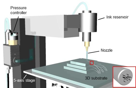
Schematic illustration of 3D printing system of stretchable metal composite. The printing system consists of a pointed nozzle connected to an ink reservoir filled with stretchable metal composite, a pressure controller, and five-axis movement stage with automatic movements in x, y, z axes and two tilting axes in the xy plane.
Credit: IBS
It seems the days are gone when just tossing a smart watch on your wrist makes you look cool. The wearable biotech industry has recently revealed its insatiable hunger for futuristic items. Pain relief goggles that monitor brain waves, vital sign monitoring stickers, and even mind reading glasses.
They are just few of the latest items discussed at the 2019 Wearable Tech, Digital Health, and Neurotech Silicon Valley conferences. Not to be sure whether all of these wearable prototypes can catch on, but one thing is clear: there are more to come in the field of wearable technology.
This great potential has been, however, held back by a technical restraint: these wearables have never really felt “wearable” to their users.
Though they were supposed to feel like a second skin of the wearer, it has been technically impossible to devise “wearable” devices that are comfortable to bend and stretch and also keep good data recording capabilities on soft and curved skin. Wearable smart devices gather a person's bio measurements by connecting electrodes to the surface of the skin.
Inside the device are 3D-shaped electrode wirings (i.e. interconnects) that transmit electrical signals. To date, not only can the wirings only be formed on a hard surface, but also the components of such interconnects delicate and hardly-stretchable metals such as gold, copper, and aluminum.
In a paper published today in the journal Nano Letters, the joint research team led by Prof. Jang-Ung Park at the Center for Nanomedicine within the Institute for Basic Science (IBS) in Daejeon, South Korea, and Prof. Chang Young Lee at the Ulsan National Institute of Science and Technology (UNIST) in Ulsan, South Korea reported fully-transformable electrode materials that also feature a high electric conductivity.
Notably, this novel composite is super-thin, 5 micrometers in diameter, which is half of the width of conventional wire bonding. By enabling ever-slimmer 3D interconnects, this study can help to revolutionize the physical appearance of smart gadgets, in addition to reinforcing their technical functions.
The research team used liquid metals (LM) as the main substrate since LMs are highly stretchable and have relatively high conductivities similar to solid metals. To improve the mechanical stability of the metal liquid, carbon nanotubes (CNT) were dispersed uniformly.
“To have a uniform and homogeneous dispersion of CNTs in liquid metal, we selected platinum (Pt), for having a strong affinity to both CNT and LM, as the mixer and it worked,” said Young-Geun Park, the first author of the study.
This study also demonstrated a new interconnection technology that can form a highly conductive 3D structure at room temperature: For having a high conductivity, the new system does not require any heating or compressing process. Also the soft and stretchable nature of the new electrode makes it easy to come through the nozzle in a fine diameter. The research team used a nozzle for the direct printing of various 3D patterning structure as shown in Figure 3. Park explains, “Forming high-conductivity 3D interconnections at room temperature is an essential technology that enables the use of various flexible electronic materials.
The wire bonding technology used in existing electronic devices forms interconnects using heat, pressure, or ultrasonic waves that can damage soft, skin-like devices. They have been a great challenge in the manufacturing process of high-performance electronic devices.” He noted that the pointed nozzle also allows reshaping of the preprinted pattern into various 3D structure, thus having an electrode work like a “switch” to turn on and off power.
Using the direct printing method, the high-resolution 3D printing of this composite forms free-standing, wire-like interconnects. This new stretchable 3D electrical interconnections specifically consist of super-thin wires, as fine as 5 micrometers. Previous studies on stretchable metals have only been able to present wire lines of several hundred micrometers in diameter.
The new system is even thinner than the interconnect of conventional wire bonding. Professor Jang-Ung Park, the corresponding author of the study noted, “We may soon be able to say goodbye to those bulky skin-based interfaces as this freely-transformable, super-thin 3D interconnection technology will come as a big breakthrough to the industry's efforts to produce ever compact and slim gadgets.”
Blurring the boundary between the human body and electric devices, this new technology will facilitate the production of more integrated and higher-performing semiconductor components for use in existing computers and smartphones, as well as for flexible and stretchable electronic devices.”


