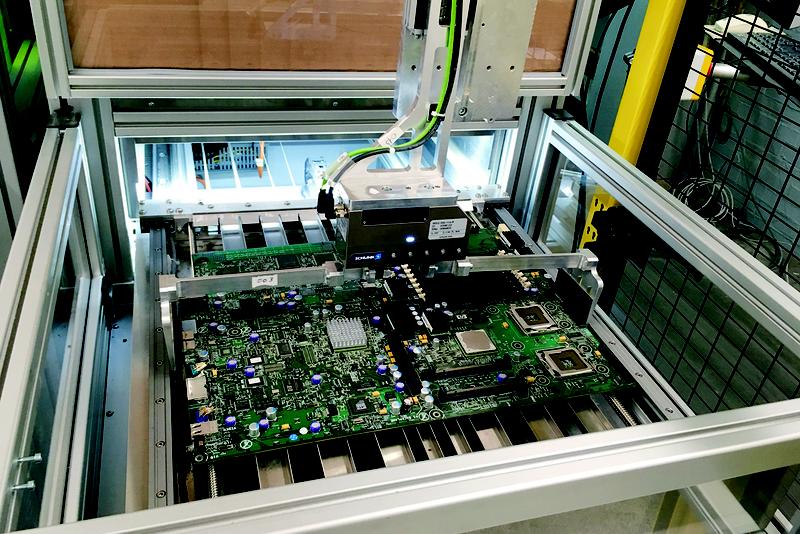

The ADIR demonstrator automatically identifies and desolders electronic components from printed circuit boards used in computers and mobile phones.
© Fraunhofer ILT, Aachen, Germany
Led by the Fraunhofer Institute for Laser Technology ILT, based in Aachen, Germany, and involving eight project partners from three countries, the ADIR project’s strategic goal is to reduce the EU’s dependency on natural resources, reduce the need for costly imports of raw materials, and demonstrate new technologies for inverse production.
The new recycling concept focuses in particular on the elements tantalum, neodymium, tungsten, cobalt and gallium. Found in virtually every modern electronic device, these metals are valuable due to their scarcity, their cost – which in some cases is close to 250 Euros per kilogram – and the tremendous difficulty of recovering them from used electronic devices in a cost-effective way.
The ADIR project consortium demonstrated the efficiency of its new recycling concept by disassembling around 1000 mobile phones and over 800 printed circuit boards from computers and presenting the results at the Berlin Recycling and Raw Materials Conference from March 2 to 3, 2020 and at the Mineral Recycling Forum on March 10, 2020 in Aachen.
Inspired by urban mining
The key term here is “urban mining”, which refers to the recovery of secondary raw materials from buildings, infrastructure or products. This increasingly important trend inspired Prof. Reinhard Noll and Dr. Cord Fricke-Begemann from Fraunhofer ILT to take a new approach to recycling.
Together with their partners in the ADIR project, they developed a concept for a piece-by-piece processing of printed circuit boards from computers and obsolete mobile phones. Support for the robotics R&D required for the project came from the Fraunhofer Institute for Factory Operation and Automation IFF in Magdeburg.
Laser plays key role
The project revolves around automated, flexible processes designed to disassemble electronic devices to selectively extract valuable component parts at the end of their useful life. The disassembly plant relies on an intelligent combination of laser technology, robotics, vision systems and information technology.
Lasers play one of the key roles, performing tasks such as identifying what each component consists of and desoldering or cutting components out of the board in a fast, non-contact process. The patented procedure is an efficient means of recovering strategically important materials of high economic value on an industrial scale.
Positive feedback motivates project partners
The project team has already received very positive feedback from experts at numerous events. This enthusiasm was particularly in evidence among attendees of the Berlin Recycling and Raw Materials Conference and the Mineral Recycling Forum in Aachen, which were held in March 2020, shortly after the project was finished.
“We’ve seen a great deal of interest from experts,” says project manager Fricke-Begemann. “And this enthusiastic response has also inspired our industry partners.” These include the company Electrocycling GmbH based in Goslar, which has been trialing the ADIR method in field tests since late 2018 and validating it for industrial use.
In a series of field campaigns, the company used the ADIR demonstrator – consisting of seven interlinked machines – to show how the developed processes can be used to extract significant quantities of tiny capacitors from electronic devices in order to recover tantalum, a valuable mineral resource. This task was carried out by the company H.C. Starck Tantalum & Niobium GmbH, which was also participating in the ADIR project.
High recycling rate for tantalum
“We disassembled around 1000 mobile phones and over 800 large computer printed circuit boards, from which we recovered several kilograms of components for recovery,” says the project manager. “We were able to gain between 96 and 98 percent of the tantalum.”
This example shows that many of the most important materials contained in electronic devices can be extracted just as efficiently as the project team had hoped, creating a novel source of secondary raw material with a high content of reusable material – significantly higher than that of the tantalum ore concentrates offered by suppliers of virgin raw material.
Database assists with automation
The pre-competitive research project has now been completed, and the ADIR team’s demonstrator has confirmed the concept’s economic viability. “The knowledge we have gained so far has already enabled us to get part of the process chain up and running,” says Professor Noll.
“This includes inspection of the printed circuit boards as well as desoldering and removal of the components.” There is still room for improvement, however, for example by using smart automation concepts to speed up the dismantling processes for the housing of mobile phones to get access to the printed circuit board, the battery and magnetic components. The researchers’ initial experiences are already being collected in a database. The data can be used by employees to train a recycling machine in processing new mobile phone models.
These ideas have already attracted interest from industry. The project team has found an initial set of partners willing to put them into practice and continues to seek further candidates. The advantages of this new concept go well beyond a more efficient use of raw materials. It has the potential to reduce Germany’s dependence on shipments of raw materials from other regions by offering new opportunities to introduce inverse production technologies. These are required to establish closed material cycles for future sustainable economy.
The ADIR project participants at project conclusion:
– Fraunhofer Institute for Laser Technology ILT, Aachen, Germany (project coordination)
– Aurubis AG, Hamburg, Germany
– Electrocycling GmbH, Goslar, Germany
– Fraunhofer Institute for Factory Operation and Automation IFF, Magdeburg, Germany
– H.C. Starck Tantalum and Niobium GmbH, Goslar, Germany
– Instytut Metali Nieżelaznych, Gliwice, Poland
– Laser Analytical Systems & Automation GmbH, Aachen, Germany
– OSAI A.S. S.p.A., Parella, Italy
– Tre Tau Engineering s.r.l., Torino, Italy
More information about the project: www.adir.eu
Dr. rer. nat. Cord Fricke-Begemann
Group Manager Material Analysis
Telephone +49 241 8906-196
cord.fricke-begemann@ilt.fraunhofer.de
apl. Prof. Dr. rer. nat. Reinhard Noll
Head of the Competence Area Measurement Technology and EUV Sources
Telephone +49 241 8906-138
reinhard.noll@ilt.fraunhofer.de
http://www.ilt.fraunhofer.de/en.html
http://www.adir.eu


