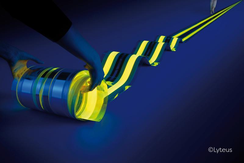
15-meter roll-to-roll device is world’s longest OLED

This 15-meter roll-to-roll device is the world’s longest OLED
© Lyteus, Picture in printable resolution: www.fep.fraunhofer.de/press
Lyteus brings together leaders in OLED technology from across Europe to create a pilot production line and product development services for OLED products.
Working together, Holst Centre and Fraunhofer FEP successfully demonstrated the possibility for continuous production of OLEDs of any length. This both reduces the cost of production and enables “cut-to-fit” lighting for applications such as transportation, architecture and interior design.
“This is a major milestone in the development of pilot line Roll-to-roll (R2R) technologies that will enable Lyteus to offer long OLED strips to its customers. It is an example of how the Lyteus pilot line turns flexible OLED possibilities into products. It was only possible due to the unique capabilities of Holst Centre and Fraunhofer FEP and the great cooperation between them and other Lyteus partners” says Pavel Kudlacek, leader of Technology Development at Lyteus.
Unique OLED structure
It is the first OLED source produced using a unique R2R process that combines the performance of an evaporated OLED stack with solution processing of auxiliary layers. Moreover, the combination improves the process reliability and enables fabrication of devices of any length.
To produce the device, Fraunhofer FEP deposited an indium-tin oxide (ITO) anode onto a protective multi-layer barrier film produced by Holst Centre. The roll was processed at Holst Centre, where slot-die coating was used to structure the anode and deposit the first layer of the OLED stack.
Fraunhofer FEP then evaporated the rest of the OLED layers and finalized the devices by lamination of Holst Centre barrier. The resulting devices have a good homogeneity and an efficacy of 15 lm/W at a light output of 1000 cd/m2.
“Roll-to-roll production promises higher volumes and lower costs for flexible electronics applications like OLEDs. At Holst Centre we have been developing a unique solution coating roll-to-roll line for 10 years. The 15-meter OLED shows that the technology is now ready for industrialization, and can deliver cost-effective, high-volume OLED production,” says Pim Groen, Program Manager at Holst Centre.
“The 15-meter OLED is further evidence of our ability to deposit high-quality organic layers and integrate them with solution-processed layers to create reliable and homogeneous devices in a continuous process. It is a step towards the creation of ‘endless’ OLED devices and a further step in our R2R OLED manufacturing processes, which we are developing now for more than 10 years,” says Jacqueline Hauptmann, Project Manager OLED R2R at Fraunhofer FEP.
About Lyteus
Lyteus offers world class capability and services in the pilot production of customised flexible OLEDs and is focusing on product streams in the areas of automotive, designer luminaires and aeronautics applications. Lyteus is a spin off from the EU-project PI-SCALE and is a cooperation between Holst Centre, Fraunhofer FEP, VTT and CPI. PI-SCALE brought together fourteen expert partners from five European countries and includes Holst Centre, Fraunhofer FEP, Centre for Process Innovation (CPI), VTT, AUDI AG, REHAU, emde development of light, Pilkington, M-Solv, FlexEnable, DuPont Teijin Films, Coatema Coating Machinery and AMIRES. PI-SCALE is an initiative of the Photonics Public Private Partnership co-funded by the European Union’s Horizon 2020 Research and Innovation Program under Grant Agreement No 688093 with a contribution of €14 million.
About Holst Centre
Established in 2005 by imec and TNO, Holst Centre is an independent R&D center that develops technologies for next-generation electronics systems. These include, but are not limited to, wireless autonomous sensors and electronic systems-in-foil that are flexible, stretchable and 3D formable. These are key building blocks for Internet of Things, mobile healthcare and smart surfaces and structures. Holst Centre bridges the gap between industry and academia by advancing technologies from lab to fab, based on robust roadmaps and programs. To facilitate this, Holst Centre establishes and creates open innovation programs involving a wide ecosystem of partners and participates in dedicated projects with industrial customers.
About Fraunhofer FEP
Fraunhofer Institute for Organic Electronics, Electron Beam and Plasma Technology FEP works on innovative solutions in the fields of vacuum coating, surface treatment as well as organic semiconductors. The core competences electron beam technology, sputtering, plasma-activated deposition and high-rate PECVD as well as technologies for the organic electronics and IC/system design provide a basis for these activities. Thus, Fraunhofer FEP offers a wide range of possibilities for research, development and pilot production, especially for the processing, sterilization, structuring and refining of surfaces as well as OLED microdisplays, organic and inorganic sensors, optical filters and flexible OLED lighting. Our aim is to seize the innovation potential of the electron beam, plasma technology and organic electronics for new production processes and devices and to make it available for our customers.
Press contact:
Ms. Annett Arnold
Fraunhofer Institute for Organic Electronics, Electron Beam and Plasma Technology FEP
Phone +49 351 2586 333 | presse@fep.fraunhofer.de
Winterbergstraße 28 | 01277 Dresden | Germany | www.fep.fraunhofer.de
http://s.fhg.de/f4N
http://www.lyteus.com
http://www.holstcentre.com
http://www.fep.fraunhofer.de


