Microchip Innovation: A Breakthrough in Laser-Driven Accelerators

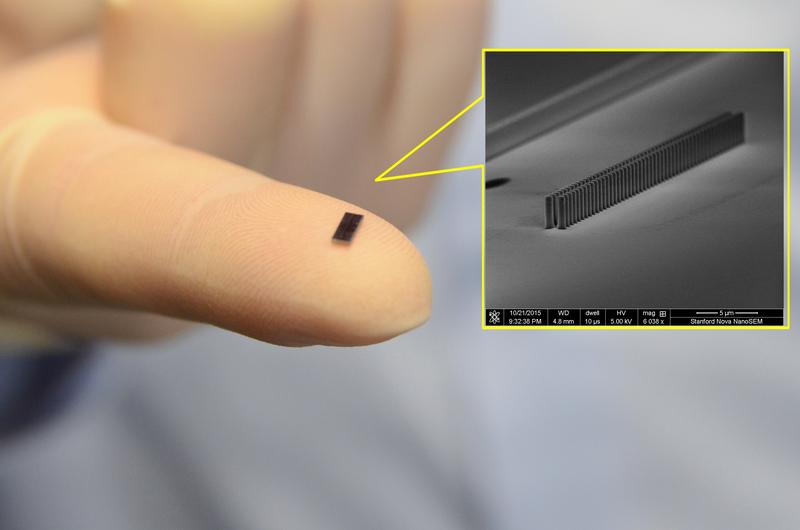
This is an accelerator chip on the tip of a finger, and an electron microscope image of the chip.
Credit: Hagen Schmidt / Andrew Ceballos
Electrical engineers in the accelerator physics group at TU Darmstadt have developed a design for a laser-driven electron accelerator so small it could be produced on a silicon chip.
It would be inexpensive and with multiple applications. The design, which has been published in Physical Review Letters, is now being realised as part of an international collaboration.
Particle accelerators are usually large and costly, but that will soon change if researchers have their way. The Accelerator on a Chip International Program (AChIP), funded by the Gordon and Betty Moore Foundation in the U.S., aims to create an electron accelerator on a silicon chip.
The fundamental idea is to replace accelerator parts made of metal with glass or silicon, and to use a laser instead of a microwave generator as an energy source.
Due to glass's higher electric field load capacity, the acceleration rate can be increased and thus the same amount of energy can be transmitted to the particles within a shorter space, making the accelerator shorter by a factor of approximately 10 than traditional accelerators delivering the same energy.
One of the challenges here is that the vacuum channel for the electrons on a chip has to be made very small, which requires that the electron beam is extremely focused. The magnetic focusing channels used in conventional accelerators are much too weak for this. This means that an entirely new focusing method has to be developed if the accelerator on a chip is to become reality.
As part of TU Darmstadt's Matter and Radiation Science profile area, the AChIP group in accelerator physics (Department of Electrical Engineering and Information Technology at TU Darmstadt), led by the junior scientist Dr. Uwe Niedermayer, recently proposed a decisive solution which calls for using the laser fields themselves to focus the electrons in a channel only 420 nanometres wide.
The concept is based on abrupt changes to the phase of the electrons relative to the laser, resulting in alternating focusing and de-focusing in the two directions in the plane of the chip surface. This creates stability in both directions.
The concept can be compared to a ball on a saddle – the ball will fall down, regardless of the direction in which the saddle tilts. However, turning the saddle continuously means the ball will remain stable on the saddle. The electrons in the channel on the chip do the same.
Perpendicular to the chip's surface, weaker focusing is sufficient, and a single quadrupole magnet encompassing the entire chip can be used. This concept is similar to that of a conventional linear accelerator. However, for an accelerator on a chip, the electron dynamics have been changed to create a two-dimensional design which can be realised using lithographic techniques from the semiconductor industry.
Niedermayer is currently a visiting scientist at Stanford University; the American university is leading the AChIP programme along with University of Erlangen in Germany. At Stanford, he is collaborating with other AChIP scientists with the aim of creating an accelerator on a chip in an experimental chamber the size of a shoebox.
A commercially available system, adapted by means of complicated non-linear optics, is used as a laser source. The aim of the AChIP programme, which has funding until 2020, is to produce electrons with one mega-electron volt of energy from the chip.
This is approximately equal to the electrical voltage of one million batteries. An additional aim is to create ultra-short (<10^-15 seconds) electron pulses, as required by the design for a scalable accelerator on a chip developed in Darmstadt.
The possible applications for an accelerator such as this would be in industry and medicine. An important long-term goal is to create a compact coherent X-ray beam source for the characterisation of materials. One example of a medical application would be an accelerator-endoscope which could be used to irradiate tumours deep within the body with electrons.
A particular advantage of this new accelerator technology is that the chips could be produced inexpensively in large numbers, which would mean that the accelerator would be within reach of the man on the street and every university could afford its own accelerator laboratory.
Additional opportunities would include the use of inexpensive coherent X-ray beam sources in photolithographic processes in the semiconductor industry, which would make a reduction in transistor size in computer processors possible, along with a greater degree of integration density.
###
The publication
Alternating-Phase Focusing for Dielectric-Laser Acceleration https:/
About TU Darmstadt
The Technische Universität (TU) Darmstadt is one of Germany's leading technical universities. TU Darmstadt incorporates diverse science cultures to create its characteristic profile. The focus is set on engineering and natural sciences, which cooperate closely with outstanding humanities and social sciences. We are enjoying a worldwide reputation for excellent research in our highly-relevant, focused profile areas: cybersecurity, internet and digitalisation, nuclear physics, fluid dynamics and heat- and mass transfer, energy systems and new materials for product innovation. We dynamically develop our portfolio of research and teaching, innovation and transfer, in order to continue opening up important opportunities for the future of society. Our 312 professors, 4,450 scientific and administrative employees and close to 26,000 students devote their talents and best efforts to this goal. Together with Goethe University Frankfurt and Johannes Gutenberg University Mainz, TU Darmstadt has formed the strategic Rhine-Main Universities alliance.
http://www.


