Light-Manipulation Breakthrough at Argonne and Harvard

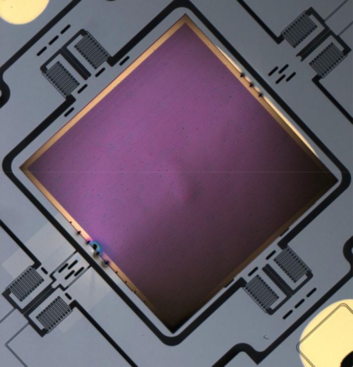
This image gives a close-up view of a metasurface-based flat lens (square piece) integrated onto a MEMS scanner. Integration of MEMS devices with metalenses will help manipulate light in sensors by combining the strengths of high-speed dynamic control and precise spatial manipulation of wave fronts.This image was taken with an optical microscope at Argonne's Center for Nanoscale Materials.
Credit: Argonne National Laboratory
In the collaborative effort between the U.S. Department of Energy's (DOE) Argonne National Laboratory and Harvard University, researchers successfully crafted a metasurface-based lens atop a Micro-Electro-Mechanical System (MEMS) platform. The result is a new infrared light-focusing system that combines the best features of both technologies while reducing the size of the optical system.
Metasurfaces can be structured at the nanoscale to work like lenses. These metalenses were pioneered by Federico Capasso, Harvard's Robert L. Wallace Professor of Applied Physics, and his group at the Harvard John A. Paulson School of Engineering and Applied Sciences (SEAS).
The lenses are rapidly finding applications because they are much thinner and less bulky than existing lenses, and can be made with the same technology used to fabricate computer chips. The MEMSs, meanwhile, are small mechanical devices that consist of tiny, movable mirrors.
“These devices are key today for many technologies. They have become technologically pervasive and have been adopted for everything from activating automobile air bags to the global positioning systems of smart phones,” said Daniel Lopez, Nanofabrication and Devices Group Leader at Argonne's Center for Nanoscale Materials, a DOE Office of Science User Facility.
Lopez, Capasso and four co-authors describe how they fabricated and tested their new device in an article in APL Photonics, titled “Dynamic metasurface lens based on MEMS technology.” The device measures 900 microns in diameter and 10 microns in thickness (a human hair is approximately 50 microns thick).
The collaboration's ongoing work to further develop novel applications for the two technologies is conducted at Argonne's Center for Nanoscale Materials, SEAS and the Harvard Center for Nanoscale Systems, which is part of the National Nanotechnology Coordinated Infrastructure.
In the technologically merged optical system, MEMS mirrors reflect scanned light, which the metalens then focuses without the need for an additional optical component such as a focusing lens. The challenge that the Argonne/Harvard team overcame was to integrate the two technologies without hurting their performance.
The eventual goal would be to fabricate all components of an optical system — the MEMS, the light source and the metasurface-based optics — with the same technology used to manufacture electronics today.
“Then, in principle, optical systems could be made as thin as credit cards,” Lopez said.
These lens-on-MEMS devices could advance the LIDAR systems used to guide self-driving cars. Current LIDAR systems, which scan for obstacles in their immediate proximity, are, by contrast, several feet in diameter.
“You need specific, big, bulky lenses, and you need mechanical objects to move them around, which is slow and expensive,” said Lopez.
“This first successful integration of metalenses and MEMS, made possible by their highly compatible technologies, will bring high speed and agility to optical systems, as well unprecedented functionalities,” said Capasso.
###
This work was also supported by the Air Force Office of Scientific Research, the National Science Foundation and the Singapore Agency for Science, Technology and Research's National Science Scholarship.
Argonne National Laboratory seeks solutions to pressing national problems in science and technology. The nation's first national laboratory, Argonne conducts leading-edge basic and applied scientific research in virtually every scientific discipline. Argonne researchers work closely with researchers from hundreds of companies, universities, and federal, state and municipal agencies to help them solve their specific problems, advance America's scientific leadership and prepare the nation for a better future. With employees from more than 60 nations, Argonne is managed by UChicago Argonne, LLC for the U.S. Department of Energy's Office of Science.
The U.S. Department of Energy's Office of Science is the single largest supporter of basic research in the physical sciences in the United States and is working to address some of the most pressing challenges of our time. For more information, visit the Office of Science website.


