New On-Silicon Laser Boosts Efficiency in Optoelectronics

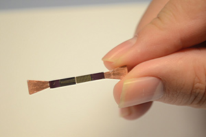
A new design for a compact on-chip laser showing the two tapered ends that allow light to be efficiently coupled with structures on the chip. © 2015 A*STAR Data Storage Institute
A compact ‘on-silicon-chip’ laser has been developed by researchers at Agency for Science, Technology and Research (A*STAR) in Singapore that boasts both excellent confinement of light for lasing and the ability to efficiently share the laser light with nearby components.
Compact lasers small enough to be integrated on chips are in great demand for a diverse range of applications, including data communication and storage. Lasers made from a combination of silicon and semiconductors containing elements from the third and fifth columns in the periodic table (dubbed III–V silicon lasers) are particularly attractive as on-chip light sources.
To be used in applications, such lasers must tightly confine light to maximize the lasing efficiency and should effectively share, or ‘couple’, light with optical waveguides — the optical equivalent of electrical wiring — located under the laser.
Jing Pu and co-workers at the A*STAR Data Storage Institute have demonstrated a III–V silicon laser that meets both criteria. Their structure realizes efficient lasing through the smart control of light — light is tightly confined to the III–V semiconductor layer in which lasing occurs. Furthermore, both laser ends are tapered to facilitate the coupling of light with underlying silicon waveguides.
“Our laser exhibits a high efficiency as well as efficient light coupling between the III–V semiconductor and silicon layers, which is the thinnest reported to date,” says Pu.
The new structure is promising as an on-chip light source for current silicon photonics technology but also as a potential new integration platform. It improves on conventional fabrication procedures, in which components are made separately and then combined, and enables fully integrated optoelectronic systems to be fabricated that take up less space on a chip.
“This new technology could replace the current approach of integrating a laser diode to an optical system through assembling and then bonding of components,” explains Pu. “The laser diodes can be fabricated exactly where they are needed, which will cut the manufacturing cost and reduce the size and weight of light sources by a factor of hundreds.”
These advantages are very attractive for many applications, including next-generation high-density magnetic data storage, where laser diodes need to be integrated on writing heads that are smaller than 0.1 square millimeters.
The team plans to improve the manufacturing process and device performance so that the technology can advance from prototype to manufacture for industrial applications. “We also aim to reduce the laser size and power consumption for use as vital components for high-performance computing,” Pu adds.
The A*STAR-affiliated researchers contributing to this research are from the Data Storage Institute. More information about the group’s research can be found at the Nanotechnology Integration Group webpage.
Reference
Pu, J., Lim, K. P., Ng, D. K. T., Krishnamurthy, V., Lee, C. W., Tang, K. et al. Heterogeneously integrated III-V laser on thin SOI with compact optical vertical interconnect access. Optics Letters 40, 1378–1381 (2015).
Associated links
Original article from A*STAR Research


