Cheers! Maxwell's electromagnetism extended to smaller scales

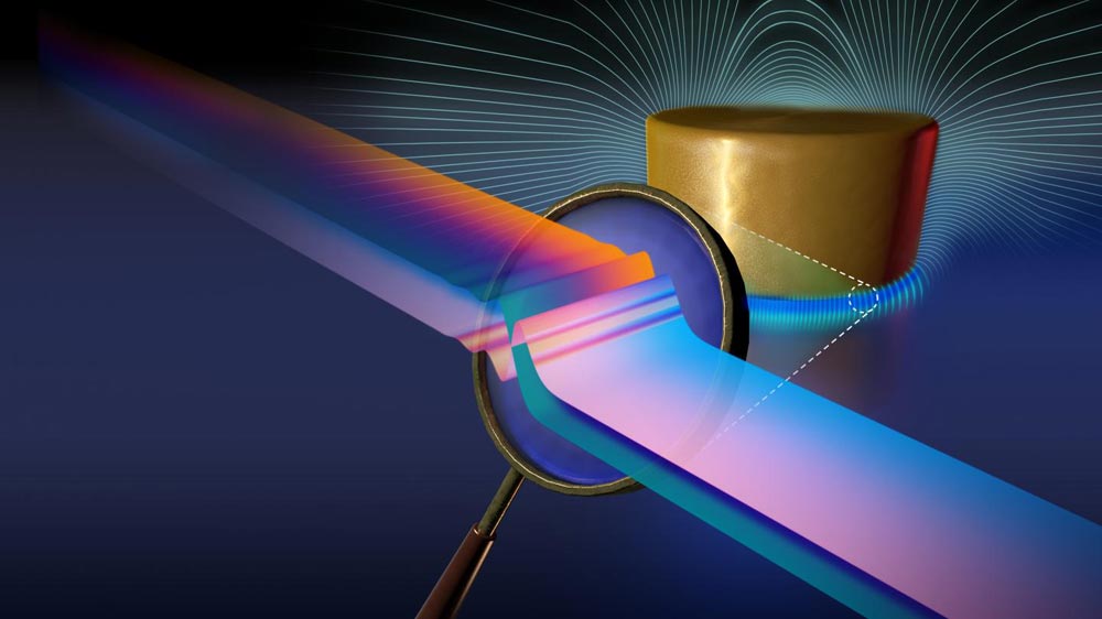
This is an artistic illustration of nonclassical effects in nanoscale electromagnetism. When the confinement of electromagnetic fields in nanostructures becomes comparable to the electronic length scales in materials, the associated nonclassical effects can substantially affect the electromagnetic response. This illustration represents a film-coupled nanodisk (the nanostructure studied in this work); the insert in the magnifier shows the electronic length scales (in this case, the 'thickness' of the surface induced charge).
Credit. Marin Soljači Research Group
It is difficult to imagine, as this treatise revolutionized our fundamental understanding of electric fields, magnetic fields, and light. The twenty original equations (nowadays elegantly reduced into four), their boundary conditions at interfaces, and the bulk electronic response functions (dielectric permittivity and magnetic permeability ) are at the root of our ability to manipulate electromagnetic fields and light (see Table (here without external interface currents or charges)).
Therefore, wondering what our life would be without Maxwell's equations means to try to envision our life without most of current science, communications and technology.
On large (macro) scales, bulk response functions and the classical boundary conditions are sufficient for describing the electromagnetic response of materials, but as we consider phenomena on smaller scales, nonclassical effects become important. A conventional treatment of classical electromagnetism fails to account for the mere existence of effects such as nonlocality [1], spill-out [2], and surface-enabled Landau damping.
Why does this powerful framework break down towards nanoscales [3]? The problem is that electronic length scales are at the heart of nonclassical phenomena, and they are not part of the classical model. Electronic length scales can be thought of as the Bohr radius or the lattice spacing in solids: small scales that are relevant for the quantum effects at hand.
Today, the path to understand and model nanoscale electromagnetic phenomena is finally open. In the breakthrough Nature paper “A General Theoretical and Experimental Framework for Nanoscale Electromagnetism”, Yang et al. [4] present a model that extends the validity of the macroscopic electromagnetism into the nano regime, bridging the scale gap.
On the theoretical side, their framework generalizes the boundary conditions by incorporating the electronic length scales in the form of so-called Feibelman d-parameters (d// and d?, see Table).
The d-parameters play a role that is analogous to that of the permittivity , but for interfaces. In terms of numerical modelling [5], all one needs to do is to pair each two-material interface with associated Feibelman d-parameters and solve the Maxwell's equations with the new boundary conditions.
On the experimental side, the authors investigate film-coupled nanoresonators, a quintessential multiscale architecture. The experimental setup was chosen because of its nonclassical nature. Even so, recently graduated postdoc and lead author Yi Yang comments: “When we built our experiment, we were lucky enough to run into the right geometry that enabled us to observe the pronounced nonclassical features, which were actually unexpected and excited everyone.
These features eventually enabled us to measure the d-parameters, which are hard to compute for some important plasmonic materials like gold (as in our case).”
The new model and experiments are momentous both for fundamental science and for diverse applications. It makes a hitherto unexplored connection between electromagnetism, material science, and condensed matter physics–one that could lead to further theoretical and experimental discoveries in all related fields, including chemistry and biology.
Application-wise, this work points to the possibility of engineering the optical response beyond the classical regime – an example would be to explore how to extract more power from emitters using antennas.
MIT Professor Marin Soljacic is enthusiastic: “We expect this work to have substantial impact. The framework we present opens a new chapter for cutting-edge nanoplasmonics–the study of optical phenomena in the nanoscale vicinity of metal surfaces–and nanophotonics–the behavior of light on the nanometer scale–and for controlling the interaction of nanometer-scale objects with light.”
###
This work was partly supported by the Army Research Office through the Institute for Soldier Nanotechnologies under contract No. W911NF-18-2-0048 and W911NF-13-D-0001, and Air Force Office of Scientific Research (AFOSR) grant under contract No. FA9550-18-1-0436. Y.Y. was partly supported by the MRSEC Program of the National Science Foundation under Grant No. DMR-1419807. D. Z. was supported by the National Science Scholarship from A*STAR, Singapore. W.Y. was supported by Programme IdEx Bordeaux-LAPHIA (Grant No. ANR-10- IDEX-03-02) and project “Resonance” (Grant No. ANR-16-CE24-0013) of the French National Agency for Research (ANR). M. Z. was supported by the National Natural Science Foundation of China (Grant No. 11574078) the China Scholarship Council. T. C. was supported by the Danish Council for Independent Research (Grant No. DFF6108-00667).
Contact information:
Marin Soljacic (soljacic@mit.ed)
Notes:
[1] the fact that optical fields affect the polarization not only at their specific point in space, but on an entire neighboring volume.
[2] the evidence that, when quantum mechanics is taken into consideration, electrons are not completely contained in solids.
[3] below 10-20 nm, the size of tens of silicon atoms in a row.
[4] A General Theoretical and Experimental Framework for Nanoscale Electromagnetism, Yi Yang, Di Zhu, Wei Yan, Akshay Agarwal, Mengjie Zheng, John D. Joannopoulos, Philippe Lalanne, Thomas Christensen, Karl K. Berggren, and Marin Soljacic. Nature, 576, 248, (2019).
[5] https:/
Written by Paola Rebusco (pao@mit.edu)
Figure Caption for artwork.png: Artistic illustration of nonclassical effects in nanoscale electromagnetism. When the confinement of electromagnetic fields in nanostructures becomes comparable to the electronic length scales in materials, the associated nonclassical effects can substantially affect the electromagnetic response. This illustration represents a film-coupled nanodisk (the nanostructure studied in this work); the insert in the magnifier shows the electronic length scales (in this case, the 'thickness' of the surface induced charge).


