Self-Assembly Breakthrough: Durable Nanocrystal Arrays Unveiled

Possible uses include biological labeling, laser light, catalysts, memory storage, and relief for physicists
A wish list for nanotechnologists might consist of a simple, inexpensive means – actually, any means at all – of self-assembling nanocrystals into robust orderly arrangements, like soup cans on a shelf or bricks in a wall, each separated from the next by an insulating layer of silicon dioxide.
The silica casing could be linked to compatible semiconductor devices. The trapped nanocrystals might function as a laser, their frequency dependent on their size, or as a very fine catalyst with unusually large surface area, or perhaps a memory device tunable by particle size and composition.
Or perhaps the technologist might want to stop nanocrystals from clumping. Agglomeration prevents them from being used as light-emitting tagging mechanisms to track cancer cells in the body and from being used in light-emitting devices needed for solid state lighting.
In this week’s journal Science, researchers at the National Nuclear Security Administration’s Sandia National Laboratories and the University of New Mexico describe a simple, commercially feasible method for doing both these things.
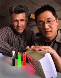
“The paper overcomes barriers to using nanocrystals routinely,” said Jeff Brinker, Sandia Fellow and UNM chemical engineering professor, who with Sandia’s Hongyou Fan led the self-assembling effort. “The question in nanotechnology isn’t ’where’s the beef,’ it’s ’where’s the connectors’? How does one make connections from the macroscale to the nanoscale? This question lies at the heart of nanotechnology.”
The self-assembly approach developed by the SNL/UNM teams allows nanocrystal arrays to be integrated into devices using standard microelectronic processing techniques, bridging huge gaps in scale.
Said IBM staff researcher Chuck Black at T. J. Watson Research Center in Yorktown Heights, NY, “One thing that’s nice is that these materials are hard materials. Often they come with an organic surfactant layer that makes it difficult to process materials, like a kind of grease. This material is embedded in oxide. It sounds like a neat thing and a new approach.” The Sandia/UNM approach scrubs the surfactants with an ozone compound.
“Also, quantum dots can be important for biolabeling and biosensing,” said Fan, who initiated the effort to use the nanocrystals for those purposes. “The beauty of our approach is that it makes these quantum dots both water-soluble and biocompatible, two essential qualities if we want to use them for in vivo imaging. The functional organic groups on the quantum dots can link with a variety of peptides, proteins, DNA, antibodies, etc. so that the dots can bind to and help locate targets like cancer cells, a critical issue in biomedicine.”
Sandia has applied for a patent on this approach, which should aid attempts at several major universities to identify individual cancer cells before they increase in number.
(Researchers have found that at the nanoscopic realm, changing merely the size of a material changes the frequency it emits when ’pumped’ by outside energy; thus, quantum dots of particular sizes and material will emit at predictable frequencies, which makes them useful adjuncts when bound to molecules created to bind to particular cancer molecules.)
The process uses a simple surfactant (similar to dishwashing soap) to surround the nanocrystals – in this case, made of gold – to make them water soluble. Further processing involving silica causes the gold nanocrystals to arrange themselves within a silica matrix in a lattice – a kind of artificial solid with properties that can be adjusted through control of nanocrystal composition, diameter, properties of the surfactant, and/or stabilizing ligands used in formation of the water soluble nanocrystals.
The robust 3-D solids, which are stable indefinitely, demonstrate the incorporation of nanocrystalline arrays into device architectures.
A further use allows physicists to go beyond modeling to determine how current scales with voltage in nanodevices. “Before,” says Brinker, “there was no way to make precisely ordered 3-D nanocrystalline solids, integrate them in devices, and characterize their behavior. There was no theoretical model. How does the current decide which way to hop between crystals?”
The new material can be used as an artificial solid to test out theories. “It should be a dream for physicists; they don’t just have to model anymore,” said Brinker.
A kind of choreographed transmission possibility exists with the so-called “coulomb blockade,” he said: No current is passed at low voltages because each crystal is separated by a thin (several nanometer thick) layer of silica dioxide, creating an insulator between the stored charges. Each nanocrystal charges separately. “This could be configured into a flash memory,” said Brinker, “with a huge number of charges stored in an array of nodes.”
Researchers at UNM’s Center for High Technology Materials performed experiments to establish the current/voltage scaling characteristics of the gold/silica arrays as a function of temperature. Sandia researcher Tim Boyle made and provided nanocrystal semiconductor (cadmium selinide) quantum dots.


