Measuring Progress in Nanotech Design

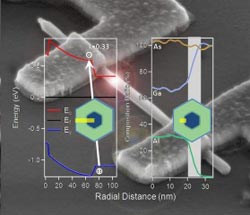
Drexel University<br><br>Key mechanisms of the measurement process are illustrated in this electron microscope image of the nanowire device.<br>
Engineers working in the nanoscale will have a new tool at their disposal thanks to an international group of researchers led by Drexel University’s College of Engineering.
This innovative procedure could alleviate the persistent challenge of measuring key features of electron behavior while designing the ever-shrinking components that allow cell phones, laptops and tablets to get increasingly thinner and more energy efficient.
“The interface between two semiconductor materials enables most of the electronic gadgets we use each day, from computers to mobile phones, displays and solar cells,” said Guannan Chen, a graduate student in Drexel’s Materials Science and Engineering department and the lead author of the group’s report, which was recently published in Nano Letters. “One of the most important features of the interface is the height of the energy step required for the electron to climb over, known as band offset. Current methods for measuring this step height in planar devices are not practical for nanoscale devices, however, so we set off to find a better way to make this measurement.”
Measuring the band offset faced by electrons jumping from one material to another is a key component of the design process because it guides the redesign and prototyping of nanoscale components in order to make them as efficient and effective as possible.
Using laser-induced current in a nanowire device and its dependence on the wavelength of the laser, the team devised a new method to derive the band offset. As they continuously change the wavelength of the laser, they measure the photocurrent responses. From this data they are able to determine the band offset.
“Using the interface within a co-axial core-shell semiconductor nanowire as a model system, we made direct measurements of the band offset for the first time in nanowire electronics,” Chen said. “This is a significant cornerstone to freely design new nanowire devices such as solar cells, LEDs, and high speed electronics for wireless communications. This work can also extend to broader material systems which can be tailored for specific application.”
The study, which was funded primarily by the National Science Foundation, also included researchers from Lehigh University, National Research Council – Institute for Microelectronics and Microsystems (IMM-CNR) and the University of Salento in Italy, Weizmann Institute of Science and Negev Nuclear Research Center in Israel and the University of Alabama. Each group added a key component to the project.
“Teamwork and close collaborations are essential in this work,” said Guan Sun, the lead researcher from Lehigh. “The smooth channel of sharing ideas and experiment resources is valuable within the team because the quality and variety of the material system is vital to achieving accurate results.”
While Drexel’s members designed the experiments, processed the materials, made the nanowire device and conducted spectroscopic experiments, Sun and Yujie Ding, from Lehigh, supported the research with complementary optical experiments.
The collaborators from the IMM-CNR, Paola Prete, and the University of Salento, Ilio Miccoli and Nico Lovergine joined forces with Hadas Shtrikman, from Weizmann Institute of Science to produce the high quality nanowire used in the testing. Patrick Kung, from the University of Alabama, analyzed the composition of the nanowire at the atomic level, and Tsachi Livneh, of Negev Nuclear Research Center, contributed to the analyses.
“This remarkably simple approach to obtaining a key characteristic in individual nanowires is an exciting advance,” said Dr. Jonathan Spanier, a professor in Drexel’s College of Engineering who is the lead investigator of the project. “We anticipate it will be a valuable method as we develop nanoscale electronic devices having completely new and important functionalities.”
With a better understanding of the material and electron behavior, the team will continue to pursue novel nanoscale optoelectronic devices such as new-concept transistors, electron-transfer devices and photovoltaic devices.
News media contacts:
Britt Faulstick, news officer, Office of University Communications, Drexel University
215-895-2617 (office), 215-796-5161 (cell), britt.faulstick@drexel.edu
Media Contact
More Information:
http://www.drexel.eduAll latest news from the category: Process Engineering
This special field revolves around processes for modifying material properties (milling, cooling), composition (filtration, distillation) and type (oxidation, hydration).
Valuable information is available on a broad range of technologies including material separation, laser processes, measuring techniques and robot engineering in addition to testing methods and coating and materials analysis processes.
Newest articles

NASA: Mystery of life’s handedness deepens
The mystery of why life uses molecules with specific orientations has deepened with a NASA-funded discovery that RNA — a key molecule thought to have potentially held the instructions for…

What are the effects of historic lithium mining on water quality?
Study reveals low levels of common contaminants but high levels of other elements in waters associated with an abandoned lithium mine. Lithium ore and mining waste from a historic lithium…

Quantum-inspired design boosts efficiency of heat-to-electricity conversion
Rice engineers take unconventional route to improving thermophotovoltaic systems. Researchers at Rice University have found a new way to improve a key element of thermophotovoltaic (TPV) systems, which convert heat…


