New industrial research technique for analyzing gallium nitride on the nanometer scale

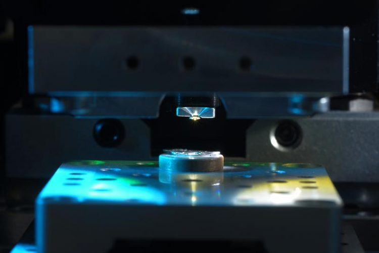
Near-field microscope with a fragment of a gallium nitride wafer. Picture Source: Fraunhofer ILT, Aachen, Germany.
The award went to three Japanese researchers who were the first to produce high-quality gallium nitride (GaN) layers and put them into series production back in 1993. Now, researchers and engineers around the world are working on analyzing and optimizing this material.
The Fraunhofer Institute for Laser Technology ILT has worked closely with RWTH Aachen University’s I. Institute of Physics (IA) to develop an analysis technology that, for the very first time, allows the structural and electronic properties of GaN and GaN composites to be studied optically on the nanometer level.
Industry’s need for mass-producible LEDs is growing, whether for smartphone, computer and TV screens or for the lighting sector. One important reason is that LEDs use many times less energy than incandescent bulbs, halogen bulbs or even energy-saving bulbs. The development of the blue LED was the last step in creating white LED light – a particularly pleasant light that significantly boosts user acceptance of the technology, for instance in home applications. Developing increasingly efficient components will rely on a quick and cost-effective analysis technique.
Optical analysis on the nanometer scale
The resolution of conventional optical microscopes reaches its physical limits when confronted with objects on the nanometer scale. Because of the light source employed, tiny structures in the nanometer range – such as those you find in modern semiconductor components – cannot be brought into focus. This rules out optical analysis techniques. Near-field microscopy circumvents this fundamental limitation and penetrates the nanometer domain to provide an optical view. This places extremely high demands on the light source used.
Aachen laser system for using near-field microscopy techniques on gallium nitride
In collaboration with fellow researchers from the Chair for Experimental Physics at RWTH Aachen University, scientists from Fraunhofer ILT have spent the past few years developing an innovative, broadband tunable laser system that is geared toward the particular requirements of semiconductor analysis. Wavelength can be adjusted to the material under inspection, which enables the new system to investigate a wide range of materials.
In contrast to the solutions available on the market to date and those employed in research and development, the new system from Aachen provides the means for much faster spectroscopic analyses. It has also opened up access to material systems that were beyond the capacities of previous systems. This includes GaN and GaN composites.
Using the new analysis system, last year the researchers in Aachen were able to obtain an optical 2D image showing tensions in the crystal structure of undoped GaN wafers for the very first time. Computer simulations helped quantify the exact extent of the tension. Recently the technique was also applied to a variety of doped GaN layers within complex structures. It’s the first time an optical technique has been available to study the structural and electronic properties of GaN and GaN composites on the nanometer scale.
Cost-effective, precise and non-destructive
Near-field microscopy offers cost and quality benefits over standard analysis techniques. The structural properties of thin GaN layers are currently studied using transmission electron microscopy; however, the costs incurred are extremely high, due in part to the laborious sample preparation process. Near-field analysis can usually be conducted without any preparation. Another benefit concerns secondary ion mass spectrometry, which is used to study the electronic properties.
Although this technique can be used to determine electronic properties along an axis at the nanometer level, it isn’t yet possible to laterally ascertain the concentration of doping atoms at a comparable resolution. The technique also damages the samples. In contrast, near-field microscopy offers nanometer-scale resolution in all dimensions. It is a completely non-destructive technique and can be implemented under normal conditions.
Potential applications for the analysis system
Near-field microscopy is suitable for a range of applications. When used in close consultation with the developers of new semiconductor components, for instance, the method can help optimize process parameters in a targeted way. The analysis also aids in the understanding of physical processes from a very early stage in development, particularly at the interfaces between the individual layers. These findings can shape subsequent development stages significantly. In high-frequency and power electronics, too, GaN is becoming more and more common as a component due to its physical properties. Near-field microscopic analysis techniques are ideally suited for researching these materials.
Contact
Dr. Fabian Gaußmann
Laser Measurement Technology
Phone +49 241 8906-489
fabian.gaussmann@ilt.fraunhofer.de
Fraunhofer Institute for Laser Technology ILT
Prof. Thomas Taubner
I. Institute of Physics (IA)
Phone +49 241 80 20260
taubner@physik.rwth-aachen.de
RWTH Aachen University
Weitere Informationen:
Media Contact
All latest news from the category: Physics and Astronomy
This area deals with the fundamental laws and building blocks of nature and how they interact, the properties and the behavior of matter, and research into space and time and their structures.
innovations-report provides in-depth reports and articles on subjects such as astrophysics, laser technologies, nuclear, quantum, particle and solid-state physics, nanotechnologies, planetary research and findings (Mars, Venus) and developments related to the Hubble Telescope.
Newest articles

A ‘language’ for ML models to predict nanopore properties
A large number of 2D materials like graphene can have nanopores – small holes formed by missing atoms through which foreign substances can pass. The properties of these nanopores dictate many…

Clinically validated, wearable ultrasound patch
… for continuous blood pressure monitoring. A team of researchers at the University of California San Diego has developed a new and improved wearable ultrasound patch for continuous and noninvasive…

A new puzzle piece for string theory research
Dr. Ksenia Fedosova from the Cluster of Excellence Mathematics Münster, along with an international research team, has proven a conjecture in string theory that physicists had proposed regarding certain equations….


