Novel crumpling method takes flat graphene from 2-D to 3-D

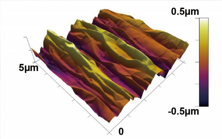
This is an atomic force microscopy image of shrink-induced crumpling/texturing of graphene. Credit: SungWoo Nam
“Fundamentally, intrinsic strains on crumpled graphene could allow modulation of electrical and optical properties of graphene,” explained SungWoo Nam, an assistant professor of mechanical science and engineering at Illinois.
“We believe that the crumpled graphene surfaces can be used as higher surface area electrodes for battery and supercapacitor applications. As a coating layer, 3D textured/crumpled nano-topographies could allow omniphobic/anti-bacterial surfaces for advanced coating applications.”
Graphene–a single atomic layer of sp2-bonded carbon atoms–has been a material of intensive research and interest over recent years. A combination of exceptional mechanical properties, high carrier mobility, thermal conductivity, and chemical inertness, make graphene a prime candidate material for next generation optoelectronic, electromechanical, and biomedical applications.
“In this study, we developed a novel method for controlled crumpling of graphene and graphite via heat-induced contractile deformation of the underlying substrate,” explained Michael Cai Wang, a graduate student and first author of the paper, “Heterogeneous, Three-Dimensional Texturing of Graphene,” which appeared in the journal Nano Letters. “While graphene intrinsically exhibits tiny ripples in ambient conditions, we created large and tunable crumpled textures in a tailored and scalable fashion.”
“As a simpler, more scalable, and spatially selective method, this texturing of graphene and graphite exploits the thermally induced transformation of shape-memory thermoplastics, which has been previously applied to microfluidic device fabrication, metallic film patterning, nanowire assembly, and robotic self-assembly applications,” added Nam, whose group has filed a patent for their novel strategy. “The thermoplastic nature of the polymeric substrate also allows for the crumpled graphene morphology to be arbitrarily re-flattened at the same elevated temperature for the crumpling process.”
“Due to the extremely low cost and ease of processing of our approach, we believe that this will be a new way to manufacture nanoscale topographies for graphene and many other 2D and thin-film materials.”
The researchers are also investigating the textured graphene surfaces for 3D sensor applications.
“Enhanced surface area will allow even more sensitive and intimate interactions with biological systems, leading to high sensitivity devices,” Nam said.
Funding for this research was provided through the Air Force Office for Scientific Research, American Chemical Society and Brain Research Foundation. In addition to Wang, co-authors from Nam's research group at Illinois include SungGyu Chun, Ryan Han, Ali Ashraf, and Pilgyu Kang.
Media Contact
All latest news from the category: Materials Sciences
Materials management deals with the research, development, manufacturing and processing of raw and industrial materials. Key aspects here are biological and medical issues, which play an increasingly important role in this field.
innovations-report offers in-depth articles related to the development and application of materials and the structure and properties of new materials.
Newest articles

NASA: Mystery of life’s handedness deepens
The mystery of why life uses molecules with specific orientations has deepened with a NASA-funded discovery that RNA — a key molecule thought to have potentially held the instructions for…

What are the effects of historic lithium mining on water quality?
Study reveals low levels of common contaminants but high levels of other elements in waters associated with an abandoned lithium mine. Lithium ore and mining waste from a historic lithium…

Quantum-inspired design boosts efficiency of heat-to-electricity conversion
Rice engineers take unconventional route to improving thermophotovoltaic systems. Researchers at Rice University have found a new way to improve a key element of thermophotovoltaic (TPV) systems, which convert heat…


