A New Kind of Wood Chip: Collaboration Could Yield Biodegradable Computer Chips

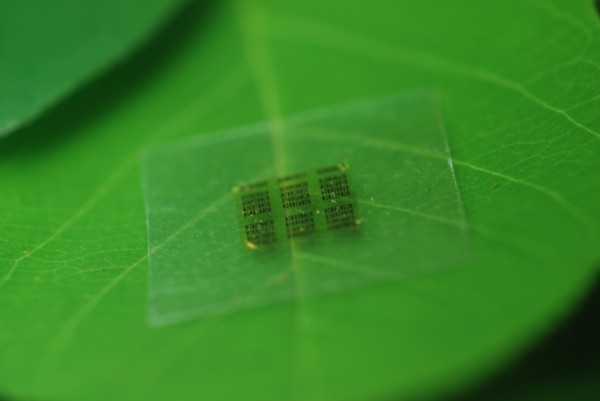
Photo: Yei Hwan Jung, Wisconsin Nano Engineering Device Laboratory A cellulose nanofibril (CNF) computer chip rests on a leaf.
Portable electronics – typically made of non-renewable, non-biodegradable and potentially toxic materials – are discarded at an alarming rate in consumers' pursuit of the next best electronic gadget.
In an effort to alleviate the environmental burden of electronic devices, a team of University of Wisconsin-Madison researchers has collaborated with researchers in the Madison-based U.S. Department of Agriculture Forest Products Laboratory (FPL) to develop a surprising solution: a semiconductor chip made almost entirely of wood.
The research team, led by UW-Madison electrical and computer engineering professor Zhenqiang “Jack” Ma, described the new device in a paper published today (May 26, 2015) by the journal Nature Communications. The paper demonstrates the feasibility of replacing the substrate, or support layer, of a computer chip, with cellulose nanofibril (CNF), a flexible, biodegradable material made from wood.
“The majority of material in a chip is support. We only use less than a couple of micrometers for everything else,” Ma says. “Now the chips are so safe you can put them in the forest and fungus will degrade it. They become as safe as fertilizer.”
Zhiyong Cai, project leader for an engineering composite science research group at FPL, has been developing sustainable nanomaterials since 2009.
“If you take a big tree and cut it down to the individual fiber, the most common product is paper. The dimension of the fiber is in the micron stage,” Cai says. “But what if we could break it down further to the nano scale? At that scale you can make this material, very strong and transparent CNF paper.”
Working with Shaoqin “Sarah” Gong, a UW-Madison professor of biomedical engineering, Cai's group addressed two key barriers to using wood-derived materials in an electronics setting: surface smoothness and thermal expansion.
“You don't want it to expand or shrink too much. Wood is a natural hydroscopic material and could attract moisture from the air and expand,” Cai says. “With an epoxy coating on the surface of the CNF, we solved both the surface smoothness and the moisture barrier.”
Gong and her students also have been studying bio-based polymers for more than a decade. CNF offers many benefits over current chip substrates, she says.
“The advantage of CNF over other polymers is that it's a bio-based material and most other polymers are petroleum-based polymers. Bio-based materials are sustainable, bio-compatible and biodegradable,” Gong says. “And, compared to other polymers, CNF actually has a relatively low thermal expansion coefficient.”
The group's work also demonstrates a more environmentally friendly process that showed performance similar to existing chips. The majority of today's wireless devices use gallium arsenide-based microwave chips due to their superior high-frequency operation and power handling capabilities. However, gallium arsenide can be environmentally toxic, particularly in the massive quantities of discarded wireless electronics.
Yei Hwan Jung, a graduate student in electrical and computer engineering and a co-author of the paper, says the new process greatly reduces the use of such expensive and potentially toxic material.
“I've made 1,500 gallium arsenide transistors in a 5-by-6 millimeter chip. Typically for a microwave chip that size, there are only eight to 40 transistors. The rest of the area is just wasted,” he says. “We take our design and put it on CNF using deterministic assembly technique, then we can put it wherever we want and make a completely functional circuit with performance comparable to existing chips.”
While the biodegradability of these materials will have a positive impact on the environment, Ma says the flexibility of the technology can lead to widespread adoption of these electronic chips.
“Mass-producing current semiconductor chips is so cheap, and it may take time for the industry to adapt to our design,” he says. “But flexible electronics are the future, and we think we're going to be well ahead of the curve.”
– John Steeno, 608-263-5988, jsteeno@wisc.edu
Contact Information
Zhenqiang “Jack” Ma, 608-261-1095, mazq@engr.wisc.edu; Zhiyong Cai, 608-231-9446, zcai@fs.fed.us
Media Contact
More Information:
http://www.wisc.eduAll latest news from the category: Information Technology
Here you can find a summary of innovations in the fields of information and data processing and up-to-date developments on IT equipment and hardware.
This area covers topics such as IT services, IT architectures, IT management and telecommunications.
Newest articles

A ‘language’ for ML models to predict nanopore properties
A large number of 2D materials like graphene can have nanopores – small holes formed by missing atoms through which foreign substances can pass. The properties of these nanopores dictate many…

Clinically validated, wearable ultrasound patch
… for continuous blood pressure monitoring. A team of researchers at the University of California San Diego has developed a new and improved wearable ultrasound patch for continuous and noninvasive…

A new puzzle piece for string theory research
Dr. Ksenia Fedosova from the Cluster of Excellence Mathematics Münster, along with an international research team, has proven a conjecture in string theory that physicists had proposed regarding certain equations….


