Could black phosphorus be the next silicon?

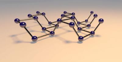
This is a schematic of the "puckered honeycomb" crystal structure of black phosphorus. Credit: Vahid Tayari/McGill University
As scientists continue to hunt for a material that will make it possible to pack more transistors on a chip, new research from McGill University and Université de Montréal adds to evidence that black phosphorus could emerge as a strong candidate.
In a study published today in Nature Communications, the researchers report that when electrons move in a phosphorus transistor, they do so only in two dimensions. The finding suggests that black phosphorus could help engineers surmount one of the big challenges for future electronics: designing energy-efficient transistors.
“Transistors work more efficiently when they are thin, with electrons moving in only two dimensions,” says Thomas Szkopek, an associate professor in McGill's Department of Electrical and Computer Engineering and senior author of the new study. “Nothing gets thinner than a single layer of atoms.”
In 2004, physicists at the University of Manchester in the U.K. first isolated and explored the remarkable properties of graphene — a one-atom-thick layer of carbon. Since then scientists have rushed to to investigate a range of other two-dimensional materials. One of those is black phosphorus, a form of phosphorus that is similar to graphite and can be separated easily into single atomic layers, known as phosphorene.
Phosphorene has sparked growing interest because it overcomes many of the challenges of using graphene in electronics. Unlike graphene, which acts like a metal, black phosphorus is a natural semiconductor: it can be readily switched on and off.
“To lower the operating voltage of transistors, and thereby reduce the heat they generate, we have to get closer and closer to designing the transistor at the atomic level,” Szkopek says. “The toolbox of the future for transistor designers will require a variety of atomic-layered materials: an ideal semiconductor, an ideal metal, and an ideal dielectric. All three components must be optimized for a well designed transistor. Black phosphorus fills the semiconducting-material role.”
The work resulted from a multidisciplinary collaboration among Szkopek's nanoelectronics research group, the nanoscience lab of McGill Physics Prof. Guillaume Gervais, and the nanostructures research group of Prof. Richard Martel in Université de Montréal's Department of Chemistry.
To examine how the electrons move in a phosphorus transistor, the researchers observed them under the influence of a magnetic field in experiments performed at the National High Magnetic Field Laboratory in Tallahassee, FL, the largest and highest-powered magnet laboratory in the world. This research “provides important insights into the fundamental physics that dictate the behavior of black phosphorus,” says Tim Murphy, DC Field Facility Director at the Florida facility.
“What's surprising in these results is that the electrons are able to be pulled into a sheet of charge which is two-dimensional, even though they occupy a volume that is several atomic layers in thickness,” Szkopek says. That finding is significant because it could potentially facilitate manufacturing the material — though at this point “no one knows how to manufacture this material on a large scale.”
“There is a great emerging interest around the world in black phosphorus,” Szkopek says. “We are still a long way from seeing atomic layer transistors in a commercial product, but we have now moved one step closer.”
###
This work was funded by the Natural Sciences and Engineering Research Council of Canada, the Canadian Institute for Advanced Research, the Fonds de recherche du Québec – Nature et technologies, Le regroupement québécois sur les matériaux de pointe, and the Canada Research Chairs program. A portion of the work was performed at the National High Magnetic Field Laboratory which is supported by the National Science Foundation, the State of Florida and the U.S. Department of Energy.
“Two-dimensional magnetotransport in a black phosphorus naked quantum well”, V. Tayari et al, published online in Nature Communications, July 7, 2015. DOI: 10.1038/ncomms8702
Contact:
Prof. Thomas Szkopek
Dept of Electrical and Computer Engineering
McGill University
thomas.szkopek@mcgill.ca
Chris Chipello
Media Relations
McGill University
514-398-4201
christopher.chipello@mcgill.ca
http://www.
http://twitter.
William Raillant-Clark
International Press Attaché
Université de Montréal
Tel.: 514 343-7593
w.raillant-clark@umontreal.ca
Media Contact
All latest news from the category: Materials Sciences
Materials management deals with the research, development, manufacturing and processing of raw and industrial materials. Key aspects here are biological and medical issues, which play an increasingly important role in this field.
innovations-report offers in-depth articles related to the development and application of materials and the structure and properties of new materials.
Newest articles

A ‘language’ for ML models to predict nanopore properties
A large number of 2D materials like graphene can have nanopores – small holes formed by missing atoms through which foreign substances can pass. The properties of these nanopores dictate many…

Clinically validated, wearable ultrasound patch
… for continuous blood pressure monitoring. A team of researchers at the University of California San Diego has developed a new and improved wearable ultrasound patch for continuous and noninvasive…

A new puzzle piece for string theory research
Dr. Ksenia Fedosova from the Cluster of Excellence Mathematics Münster, along with an international research team, has proven a conjecture in string theory that physicists had proposed regarding certain equations….


