Ideal size for computer memory

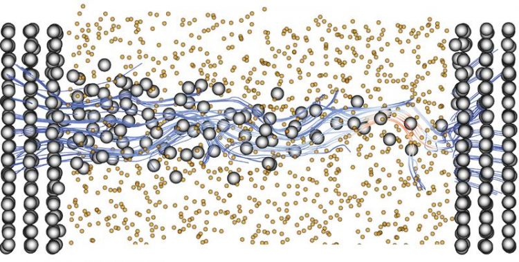
Atomic-scale computer simulation of a CBRAM cell subjected to 1mV voltage: electron trajectories (blue and red lines); copper atoms (grey); silicon and oxygen atoms (orange). © Mathieu Luisier / ETH Zurich
CBRAM (conductive bridging random access memory) could play a fundamental role in memory in the future by storing data in a non-volatile (i.e., near-permanent) way. To reduce the size and power consumption of such components, it is essential to precisely understand their behaviour at the atomic level.
Mathieu Luisier, associate professor at ETH Zurich, and his team studied this type of memory, which consists of two metal electrodes separated by an insulator. The researchers developed a computer model of a CBRAM that consists of some 4500 atoms and obeys the laws of quantum mechanics governing the microscopic world. This atomic-scale simulation makes it possible to precisely describe the intensity of the current generated by a metallic nanofilament as it forms and dissolves between the electrodes.
Ten atoms thick
“This is a huge step forward”, says Mathieu Luisier, who was an SNSF professor at ETH Zurich from 2011 to 2016. “Up to now, existing models could handle only about a hundred atoms.” The new model accurately reproduces the electric current as well as the energy dissipated by the cell, in turn enabling calculation of its temperature.
The researchers are able to observe the effect of changes in the thickness of the insulator and the diameter of the metallic filament. The findings, which were presented at the IEDM conference in San Francisco in December 2017, show that local power consumption and heat are reduced if the two electrodes are moved closer together.(*) But only up to a certain point: electrodes that are too close are subject to the quantum tunneling effect, and the current between them is no longer controllable.
The research shows that in an optimal CBRAM geometry, the insulator is 1.5 to 2 nanometers (about 10 atoms) thick. Fabrication is still a challenge, however: machines capable of achieving such dimensions use a thermal probe lithography technique that is currently ill suited to mass production. “Today, a typical CMOS-type transistor channel measures about 20 nanometres, or ten times thicker than the CBRAM insulators we investigated”, says Luisier. Consequently, Moore's law – which predicts that the size of electronic components will halve every 18–24 months – could run up against a wall within a decade.
To achieve their 4500-atom model, the researchers benefited from access to the world's third-most-powerful computer – Piz Daint – which is located at the Swiss National Supercomputing Centre (CSCS) in Lugano and can perform up to 20 million billion operations per second. This type of study requires 230 state-of-the-art graphics cards; Piz Daint has more than 4000 of them. Each card has its own CPU. “Even with this computational power, it takes ten hours or so to simulate one memory and to determine its electrical characteristics”, says Luisier.
(*) F. Ducry et al.: Ab-initio Modeling of CBRAM Cells: from Ballistic Transport Properties to Electro-Thermal Effects. Proceedings of the IEDM Conference 2017.
This research was funded by the SNSF, the Werner Siemens Foundation an ETH Research Grant as well as the Swiss National Supercomputing Centre (CSCS).
Promoting young Researchers
The SNSF has launched a new funding scheme to support researchers working towards a professorship. SNSF Eccellenza Grants allow tenure-track assistant professors to form a new research team and lead an ambitious scientific project. SNSF Eccellenza Professorial Fellowships cover the salaries of assistant professors as well as their project costs. The new scheme replaces the SNSF professorship grant, which has supported 691 researchers since its launch in 2000. And it has done so with great success: approx. 80% of grantees went on to obtain a professorship at a higher education institution in Switzerland or abroad.
Contact
Prof. Mathieu Luisier
Integrated Systems Laboratory
ETH Zurich
CH-8092 Zurich
Telephone: +41 44 632 53 53 or +41 79 454 93 78
E-mail: mluisier@iis.ee.ethz.ch
http://www.snf.ch/en/researchinFocus/newsroom/Pages/news-171204-press-release-id…
https://iis-people.ee.ethz.ch/~mluisier/iedm_abstract_ducry.pdf
http://www.snf.ch/en/funding/careers/eccellenza/Pages/default.aspx
http://p3.snf.ch/Project-159314 'Project: Physics-based Modeling of Electronic Devices at the Nanometer Scale'
Media Contact
All latest news from the category: Information Technology
Here you can find a summary of innovations in the fields of information and data processing and up-to-date developments on IT equipment and hardware.
This area covers topics such as IT services, IT architectures, IT management and telecommunications.
Newest articles

A ‘language’ for ML models to predict nanopore properties
A large number of 2D materials like graphene can have nanopores – small holes formed by missing atoms through which foreign substances can pass. The properties of these nanopores dictate many…

Clinically validated, wearable ultrasound patch
… for continuous blood pressure monitoring. A team of researchers at the University of California San Diego has developed a new and improved wearable ultrasound patch for continuous and noninvasive…

A new puzzle piece for string theory research
Dr. Ksenia Fedosova from the Cluster of Excellence Mathematics Münster, along with an international research team, has proven a conjecture in string theory that physicists had proposed regarding certain equations….


