NUST MISIS scientists manage to observe the inner structure of photonic crystals

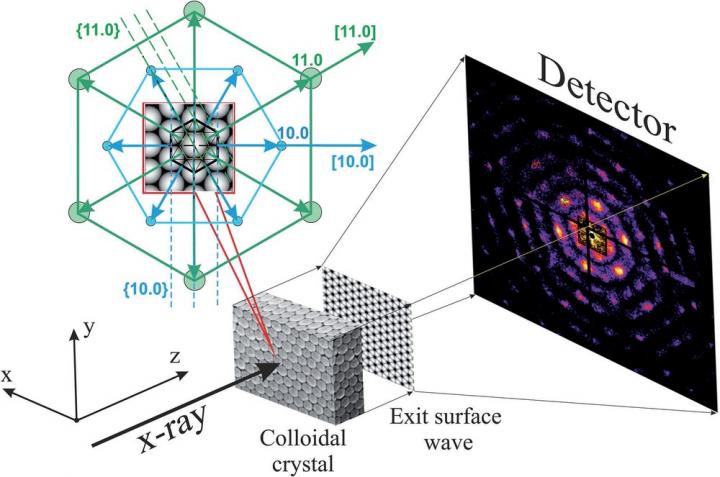
This is the scheme of analysis of photonic crystals' inner structure with the help of ptychography. Credit: ©NUST MISIS
With the help of electronic microcopy, scientists have managed to track defects in the surface of two-dimensional photonic crystals, but there was a problem with bulk photonic crystals. There was no way for scientists to research the inner parts of these unusual crystals, in which the order occurred at a tenth of a nanometer, or even in substances — the order arose at a tenth and a hundredth of a nanometer. Hence, scientists have been searching for a method to better measure these crystals for some time.
“Ilya Besedin, an engineer from the NUST MISIS Laboratory of Superconducting Metamaterials, jointly with a group of scientists from Germany, the Netherlands, and Russia, for the first time, has demonstrated that there is a method of non-destructive analysis of the inner structure of the substance, which cannot be seen with the use of conventional X-rays. The new system will help to create microprocessors for optical computers. It`s not a coincidence that the work was published in Small journal, one of the most cited journals in the field of biotechnologies, biomaterials, and interdisciplinary engineering”, said Alevtina Chernikova, Rector of NUST MISIS.
As Ilya Besedin stated, their research group led by Professor Ivan Vartanyants from MEPhI has applied the recently developed method of ptychographic to photonic crystals. The method's essence is that the substance is illuminated by x-ray radiation of an exactly defined wave (coherent). Sources of such radiation are called synchrotrons, and their experiments were conducted during the third generation synchrotron commissioned to research particle physics in Germany (DESY).
“With conventional x-rays you can scan either macroscopic or very ordered structures. In our case, for structures of polystyrene spheres of an almost micron size, the accuracy of the image will be even worse than in fluoroscopy. At least, it won`t be possible to discern a single object [smaller] than a micron”, said Ilya Besedin.
Comparing fire and led is a good analogy to understand the difference in the quality of conventional x-rays and synchrotron. Fire ignites in a wide range of frequencies while led ignites on a strictly determined frequency and in a given direction. Thanks to such a high quality x-ray, Ilya Besedin and his colleagues have managed to “observe” through the mesoscopic structure the structures of substances where the sequence is found only at a distance of tens and hundreds of nanometers. Most importantly, scientists have managed to identify internal defects of mesoscopic structures.
As Ilya Besedin explained, if the crystal is perfect, the beam can pass through or be reflected. However, because of defects, the beam might deviate from a straight line.
“By knowing information about packaging defects, we can understand the logic through which the beam changes its direction. This means we can try to collect logical designs based on photonic crystals. Another thing is that we are not able to control the formation of these defects, we can only try to reduce [the defects] at the macro level”, explained Besedin.
“A photonic crystal is like a waveguide for the light, only better. The waveguide is almost impossible to bend, and it's impossible to create photonic microchips on waveguides. A photonic crystal is most suitable for the creation of integral optical microchips where the light can spread where the developers need it to”, noted Ilya Besedin.
According to him this is why the main value of this work is in the analysis of photonic crystals` inner structure with the help of ptychography.
“We have shown that now, with the help of x-rays, we can observe defects in periodic mesoscopic structures. The next stage of specification is to expose these structures to radiation with an x-ray laser. This can give a more accurate picture of the internal structure, but there are also some difficulties. The laser beam is, by definition, more powerful than just an outgoing one from synchrotron. While increasing the power, the probability of destroying the investigated structure increases significantly, which is not [good]. Ptychography also allows researchers to study the inner structure of a crystal without destroying it. That is why such a method will definitely find its application”, Besedin concluded.
Media Contact
All latest news from the category: Materials Sciences
Materials management deals with the research, development, manufacturing and processing of raw and industrial materials. Key aspects here are biological and medical issues, which play an increasingly important role in this field.
innovations-report offers in-depth articles related to the development and application of materials and the structure and properties of new materials.
Newest articles

A new puzzle piece for string theory research
Dr. Ksenia Fedosova from the Cluster of Excellence Mathematics Münster, along with an international research team, has proven a conjecture in string theory that physicists had proposed regarding certain equations….

Climate change can cause stress in herring larvae
The occurrence of multiple stressors undermines the acclimatisation strategies of juvenile herring: If larvae are exposed to several stress factors at the same time, their ability to respond to these…

Making high-yielding rice affordable and sustainable
Plant biologists show how two genes work together to trigger embryo formation in rice. Rice is a staple food crop for more than half the world’s population, but most farmers…


