Cell membrane inspires new ultrathin electronic film

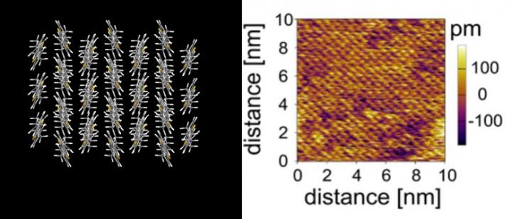
Top surface view of 3-D computer model (left) and Atomic Force Microscopy image (right) of the new film made by University of Tokyo scientists. The well-organized structure of the molecules is visible in both the 3-D computer model and microscope image as a herringbone or cross-hair pattern. The color differences in the microscopy image are a result of the different lengths of the molecules' tails; the length differences cause the geometric frustration that prevents layers from stacking. pm = picometers, nm = nanometers. Credit: Shunto Arai and Tatsuo Hasegawa
“We want to give electronic devices the features of real cell membranes: flexible, strong, sensitive, and super thin. We found a novel way to design semiconductive single molecular bilayers that allows us to manufacture large surface areas, up to 100 square centimeters (39 square inches). They can function as high performance thin film transistors and could have many applications in the future,” said Assistant Professor Shunto Arai, the first author on the recent research publication.
Professor Tatsuo Hasegawa of the University of Tokyo Department of Applied Physics led the team that built the new film. The breakthrough responsible for their success is a concept called geometric frustration, which uses a molecular shape that makes it difficult for molecules to settle in multiple layers on top of each other.
The film is transparent, but the forces of attraction and repulsion between the molecules create an organized, repeated herringbone pattern when the film is viewed from above through a microscope. The overall molecular structure of the bilayer is highly stable. Researchers believe it should be possible to build the same structure out of different molecules with different functionalities.
The individual molecules used in the current film are divided into two regions: a head and a tail. The head of one molecule stacks on top of another, with their tails pointing in opposite directions so the molecules form a vertical line. These two molecules are surrounded by identical head-to-head pairs of molecules, which all together form a sandwich called a molecular bilayer.
Researchers discovered they could prevent additional bilayers from stacking on top by building the bilayer out of molecules with different length tails, so the surfaces of the bilayer are rough and naturally discourage stacking. This effect of different lengths is referred to as geometric frustration.
Standard methods of creating semiconductive molecular bilayers cannot control the thickness without causing cracks or an irregular surface. The geometric frustration of different length tails has allowed researchers to avoid these pitfalls and build a 10cm by 10cm (3.9 inches by 3.9 inches) square of their film using the common industrial method of solution processing.
The semiconductive properties of the bilayer may give the films applications in flexible electronics or chemical detection.
Semiconductors are able to switch between states that allow electricity to flow (conductors) and states that prevent electricity from flowing (insulators). This on-off switching is what allows transistors to quickly change displayed images, such as a picture on an LCD screen. The single molecular bilayer created by the UTokyo team is much faster than amorphous silicon thin film transistors, a common type of semiconductor currently used in electronics.
The team will continue to investigate the properties of geometrically frustrated single molecular bilayers and potential applications for chemical detection. Collaborators based at the National Institute of Advanced Industrial Science and Technology, the Nippon Kayaku Company Limited, Condensed Matter Research Center, and High Energy Accelerator Research Organization also contributed to the research.
###
Journal Article
Shunto Arai, Satoru Inoue, Takamasa Hamai, Reiji Kumai, Tatsuo Hasegawa. 2018. “Semiconductive single molecular bilayers realized using geometrical frustration.” Adv. Mater., 30, DOI: 10.1002/adma.201707256 https:/
Related Links
Hasegawa Group Lab Websites
University of Tokyo: http://hsgw.
National Institute of Advanced Industrial Science and Technology (AIST): https:/
Research Contact
Professor Tatsuo Hasegawa
Graduate School of Engineering, Department of Applied Physics, University of Tokyo
7-3-1 Hongo, Bunkyo-ku, Tokyo 113-8656 JAPAN
E-mail: t-hasegawa ap.t.u-tokyo.ac.jp
Phone: +81-3-5841-6841
Assistant Professor Shunto Arai
Graduate School of Engineering, Department of Applied Physics, University of Tokyo
7-3-1 Hongo, Bunkyo-ku, Tokyo 113-8656 JAPAN
E-mail: arai ap.t.u-tokyo.ac.jp
Phone: +81-3-5841-7757
Public Relations Contact
Ms. Yayoi Miyagawa
Public Relations Office, Graduate School of Engineering, University of Tokyo
7-3-1 Hongo, Bunkyo-ku, Tokyo 113-8656 JAPAN
Tel: +81-3-5841-1790
Fax: +81-3-5841-0529
Email: kouhou@pr.t.u-tokyo.ac.jp
About the University of Tokyo
The University of Tokyo is Japan's leading university and one of the world's top research universities. The vast research output of some 6,000 researchers is published in the world's top journals across the arts and sciences. Our vibrant student body of around 15,000 undergraduate and 15,000 graduate students includes over 2,000 international students. Find out more at http://www.
Media Contact
All latest news from the category: Power and Electrical Engineering
This topic covers issues related to energy generation, conversion, transportation and consumption and how the industry is addressing the challenge of energy efficiency in general.
innovations-report provides in-depth and informative reports and articles on subjects ranging from wind energy, fuel cell technology, solar energy, geothermal energy, petroleum, gas, nuclear engineering, alternative energy and energy efficiency to fusion, hydrogen and superconductor technologies.
Newest articles

A ‘language’ for ML models to predict nanopore properties
A large number of 2D materials like graphene can have nanopores – small holes formed by missing atoms through which foreign substances can pass. The properties of these nanopores dictate many…

Clinically validated, wearable ultrasound patch
… for continuous blood pressure monitoring. A team of researchers at the University of California San Diego has developed a new and improved wearable ultrasound patch for continuous and noninvasive…

A new puzzle piece for string theory research
Dr. Ksenia Fedosova from the Cluster of Excellence Mathematics Münster, along with an international research team, has proven a conjecture in string theory that physicists had proposed regarding certain equations….


