The holy grail of nanowire production

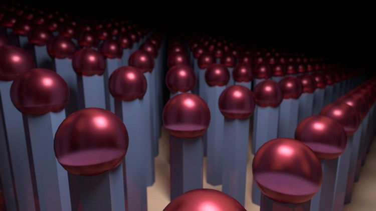
EPFL researchers have found a way to control and standardize the production of nanowires on silicon surfaces. This discovery could make it possible to grow nanowires on electronic platforms, with potential applications including the integration of nanolasers into electronic chips and improved energy conversion in solar panels. Credit: Jamani Caillet / EPFL
They can emit, concentrate and absorb light and could therefore be used to add optical functionalities to electronic chips.
They could, for example, make it possible to generate lasers directly on silicon chips and to integrate single-photon emitters for coding purposes. They could even be applied in solar panels to improve how sunlight is converted into electrical energy.
Up until now, it was impossible to reproduce the process of growing nanowires on silicon semiconductors – there was no way to repeatedly produce homogeneous nanowires in specific positions.
But researchers from EPFL's Laboratory of Semiconductor Materials, run by Anna Fontcuberta i Morral, together with colleagues from MIT and the IOFFE Institute, have come up with a way of growing nanowire networks in a highly controlled and fully reproducible manner.
The key was to understand what happens at the onset of nanowire growth, which goes against currently accepted theories. Their work has been published in Nature Communications.
“We think that this discovery will make it possible to realistically integrate a series of nanowires on silicon substrates,” says Fontcuberta i Morral. “Up to now, these nanowires had to be grown individually, and the process couldn't be reproduced.”
Getting the right ratio
The standard process for producing nanowires is to make tiny holes in silicon monoxide and fill them with a nanodrop of liquid gallium. This substance then solidifies when it comes into contact with arsenic.
But with this process, the substance tends to harden at the corners of the nanoholes, which means that the angle at which the nanowires will grow can't be predicted. The search was on for a way to produce homogeneous nanowires and control their position.
Research aimed at controlling the production process has tended to focus on the diameter of the hole, but this approach has not paid off. Now EPFL researchers have shown that by altering the diameter-to-height ratio of the hole, they can perfectly control how the nanowires grow. At the right ratio, the substance will solidify in a ring around the edge of the hole, which prevents the nanowires from growing at a non-perpendicular angle. And the researchers' process should work for all types of nanowires.
“It's kind of like growing a plant. They need water and sunlight, but you have to get the quantities right,” says Fontcuberta i Morral.
This new production technique will be a boon for nanowire research, and further samples should soon be developed.
###
Source: J. Vukajlovic-Plestina, W. Kim, L. Ghisalberti, G. Varnavides, G. Tütüncuoglu, H. Potts, M. Friedl, L. Güniat, W. C. Carter, V. G. Dubrovskii, A. Fontcuberta i Morral, Fundamental aspects to localize self-catalyzed III-V nanowires on silicon, Nature Communications
Media Contact
More Information:
http://dx.doi.org/10.1038/s41467-019-08807-9All latest news from the category: Power and Electrical Engineering
This topic covers issues related to energy generation, conversion, transportation and consumption and how the industry is addressing the challenge of energy efficiency in general.
innovations-report provides in-depth and informative reports and articles on subjects ranging from wind energy, fuel cell technology, solar energy, geothermal energy, petroleum, gas, nuclear engineering, alternative energy and energy efficiency to fusion, hydrogen and superconductor technologies.
Newest articles

A ‘language’ for ML models to predict nanopore properties
A large number of 2D materials like graphene can have nanopores – small holes formed by missing atoms through which foreign substances can pass. The properties of these nanopores dictate many…

Clinically validated, wearable ultrasound patch
… for continuous blood pressure monitoring. A team of researchers at the University of California San Diego has developed a new and improved wearable ultrasound patch for continuous and noninvasive…

A new puzzle piece for string theory research
Dr. Ksenia Fedosova from the Cluster of Excellence Mathematics Münster, along with an international research team, has proven a conjecture in string theory that physicists had proposed regarding certain equations….


