Organic electronics: a new semiconductor in the carbon-nitride family

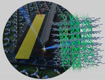
The illustration is alluding to the laser experiment in the background and shows the structure of TGCN. Credit: C. Merschjann/HZB
A team headed by chemist Dr. Michael J. Bojdys at Humboldt University Berlin recently synthesised a new organic semiconductor material in the carbon-nitride family. Triazine-based graphitic carbon nitride (or TGCN) consists of only carbon and nitrogen atoms, and can be grown as a brown film on a quartz substrate.
The combination of C and N atoms form hexagonal honeycombs similar to graphene, which consists of pure carbon.Just as with graphene, the crystalline structure of TGCN is two-dimensional. With graphene, however, the planar conductivity is excellent, while its perpendicular conductivity is very poor.
In TGCN it is exactly the opposite: the perpendicular conductivity is about 65 times greater than the planar conductivity. With a band gap of 1.7 electron volts, TGCN is a good candidate for applications in optoelectronics.
HZB physicist Dr. Christoph Merschjann subsequently investigated the charge transport properties in TGCN samples using time-resolved absorption measurements in the femto- to nanosecond range at the JULiq laser laboratory, a JointLab between HZB and Freie Universität Berlin.
These kinds of laser experiments make it possible to connect macroscopic electrical conductivity with theoretical models and simulations of microscopic charge transport. From this approach he was able to deduce how the charge carriers travel through the material.
“They do not exit the hexagonal honeycombs of triazine horizontally, but instead move diagonally to the next hexagon of triazine in the neighbouring plane. They move along tubular channels through the crystal structure.”
This mechanism might explain why the electrical conductivity perpendicular to the planes is considerably higher than that along the planes. However, this is probably not sufficient to explain the actual measured factor of 65.
“We do not yet fully understand the charge transport properties in this material and want to investigate them further”, adds Merschjann. At ULLAS / HZB in Wannsee, the analysis lab used subsequent to JULiq, the setup is being prepared for new experiments to accomplish this.
“TGCN is therefore the best candidate so far for replacing common inorganic semiconductors like silicon and their crucial dopants, some of which are rare elements”, says Bojdys. “The fabrication process we developed in my group at Humboldt-Universität, produces flat layers of semiconducting TGCN on an insulating quartz substrate. This facilitates upscaling and simple fabrication of electronic devices.”
Media Contact
All latest news from the category: Materials Sciences
Materials management deals with the research, development, manufacturing and processing of raw and industrial materials. Key aspects here are biological and medical issues, which play an increasingly important role in this field.
innovations-report offers in-depth articles related to the development and application of materials and the structure and properties of new materials.
Newest articles

Innovative vortex beam technology
…unleashes ultra-secure, high-capacity data transmission. Scientists have developed a breakthrough optical technology that could dramatically enhance the capacity and security of data transmission (Fig. 1). By utilizing a new type…

Tiny dancers: Scientists synchronise bacterial motion
Researchers at TU Delft have discovered that E. coli bacteria can synchronise their movements, creating order in seemingly random biological systems. By trapping individual bacteria in micro-engineered circular cavities and…

Primary investigation on ram-rotor detonation engine
Detonation is a supersonic combustion wave, characterized by a shock wave driven by the energy release from closely coupled chemical reactions. It is a typical form of pressure gain combustion,…


