Printed miniature loudspeaker listening into the future

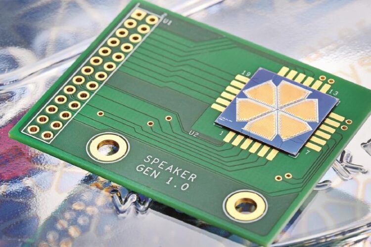
Hexagonal, tiny, inexpensive: The mini loudspeaker from Fraunhofer ILT, Fraunhofer ISIT and IWE2 at RWTH Aachen University proves that microactuators can be produced in seconds and at low costs using inkjet printers and lasers.
© Fraunhofer ILT, Aachen, Germany
In an additive manufacturing process, miniature loudspeakers can be produced efficiently and cost-effectively as part of piezoelectric microelectromechanical systems – so-called piezo-MEMS – using a combination of inkjet printing and laser technology. This has been demonstrated by scientists at the Fraunhofer Institute for Laser Technology ILT, the Institute for Materials in Electrical Engineering 2 (IWE2) at RWTH Aachen University and the Fraunhofer Institute for Silicon Technology ISIT. The partners manufactured a corresponding demo component as part of the recently completed BMBF joint project »Generative Manufacturing of Efficient Piezo-MEMS for Microactuators (GENERATOR)«.
Piezo-MEMS are true technical all-rounders because the ultra-thin piezoelectric layers fulfill actuator or sensor functions: Either they expand when an electric field is applied or they convert mechanical motion into electrical voltage. Accordingly, they are in demand in communications or medical technology, for example, as sensors or actuators in pumps, valves or loudspeakers – in each case in miniature format. The thin films are usually made of lead zirconate titanate (PZT), currently the most powerful and functional piezoelectric ceramic. Preferably, piezoelectric layers with a thickness of a few μm are used, which can be structured very precisely by etching or direct printing, for example.
Laser-assisted printing processes as an alternative to conventional high-vacuum coating

© Fraunhofer ILT, Aachen, Germany
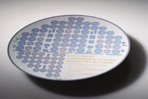
Until now, conventional vacuum and mask-based manufacturing methods have been used to produce piezo-MEMS, but these methods are very time-consuming and cost-intensive, especially for the manufacture of small batches. As part of the GENERATOR project, funded by the German Federal Ministry of Education and Research (BMBF), Fraunhofer ILT, together with Fraunhofer ISIT and IWE2 of RWTH Aachen University, therefore, developed a process combination of digital inkjet printing and laser crystallization as a favorable alternative: After PZT special ink is applied to 8” silicon wafers, crystallization follows by means of laser radiation at local temperatures of over 700 °C. Quality is ensured by a temperature-controlled process that limits temperature fluctuations to ± 5 °C.
Trend towards multi-material stack
A multilayer actuator with a total layer thickness of 2 to 3 µm was built out of several 20 to 30 nm thin PZT layers. “Initially, we only applied a single layer, but now a multi-material stack can be created layer by layer,” explains Fraunhofer ILT scientist Samuel Fink. Alternately, a total of up to 30 layers of functional ceramics and electrodes can be built on top of each other to form a micro loudspeaker. Thanks to this design, the actuator is said to offer better performance and higher reproduction quality than conventional actuators. The PZT layers and electrode layers interlock like two very fine combs. The fast laser processing of the layers reduces the processing time per layer, which would otherwise take minutes, down to just a few seconds. Instead of the common and very expensive platinum, the scientists use the electrically conductive ceramic lanthanum nickel oxide (LNO) as the electrode material. By dispensing with metallic components, they can significantly increase the durability of these purely ceramic multi-material stacks and reduce material costs at the same time.
If an AC voltage is applied to this multi-material stack, the PZT layers deform in fractions of a second, thereby exciting the entire stack to vibrate. Since the entire system is only a few µm thick and, thus, has a very low mass, acoustic signals can be transmitted excellently, especially in the high-frequency range. “The beauty of this manufacturing method is the digitally controllable printing and laser processes, which allow instantaneous design changes of the manufactured layers without additional costs for masks or tools and thus also the production of smaller batch sizes,” says Dr. Christian Vedder, head of the Thin Film Processing group at Fraunhofer ILT.
Opportunity for small and medium-sized enterprises
Conventional systems for manufacturing thin-film electronics cost several million euros and only make financial sense for large-scale production. For smaller batch sizes, the additive hybrid process becomes attractive, especially if the component consists of several layers like the micro loudspeaker. The process is, therefore, particularly suitable for small and medium-sized enterprises (SMEs), because their investment in the system technology turns out to be significantly less than that of conventional technology. Fink: “The user needs appropriate printing and laser system technology as well as specially adapted PZT and LNO inks. Even very small job stores could, therefore, set up small-scale production for microactuators in the future.”
It can be done easier: glass instead of silicon
Until now, the process has been used to coat silicon substrates. These substrates have had to undergo relatively complex post-processing after the multi-stack system has been built in order to produce components that are ready for use. However, the properties of the laser-based manufacturing process mean that other substrates such as ultra-thin glass could also conceivably be used, an advantage that would simplify production even further and open up a wide range of possible applications. “In the course of the project, in addition to process development, we were able to produce very exciting results on the fundamental mechanisms of laser crystallization of ceramics, which take place in the millisecond range. New possibilities are emerging here that are of great interest to me personally and will hopefully soon be transferred to other materials and thus areas of application,” says Fink, looking to the future.
The project underlying this report was funded by the German Federal Ministry of Education and Research under grant number 03VP02223.
Wissenschaftliche Ansprechpartner:
Samuel Fink M. Sc.
Group Thin Film Processing
Telephone +49 241 8906-624
samuel.fink@ilt.fraunhofer.de
Dr.-Ing. Christian Vedder
Group Leader Thin Film Processing
Telephone +49 241 8906-378
christian.vedder@ilt.fraunhofer.de
Weitere Informationen:
Media Contact
All latest news from the category: Power and Electrical Engineering
This topic covers issues related to energy generation, conversion, transportation and consumption and how the industry is addressing the challenge of energy efficiency in general.
innovations-report provides in-depth and informative reports and articles on subjects ranging from wind energy, fuel cell technology, solar energy, geothermal energy, petroleum, gas, nuclear engineering, alternative energy and energy efficiency to fusion, hydrogen and superconductor technologies.
Newest articles

Compact LCOS Microdisplay with Fast CMOS Backplane
…for High-Speed Light Modulation. Researchers from the Fraunhofer Institute for Photonic Microsystems IPMS, in collaboration with HOLOEYE Photonics AG, have developed a compact LCOS microdisplay with high refresh rates that…

New perspectives for material detection
CRC MARIE enters third funding period: A major success for terahertz research: Scientists at the University of Duisburg-Essen and the Ruhr University Bochum have been researching mobile material detection since…

CD Laboratory at TU Graz Researches New Semiconductor Materials
Using energy- and resource-saving methods, a research team at the Institute of Inorganic Chemistry at TU Graz aims to produce high-quality doped silicon layers for the electronics and solar industries….


