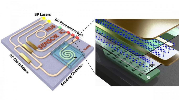
Black phosphorus future in 3D analysis, molecular fingerprinting

Schematics of an on-chip mid-infrared system based on black phosphorus-silicon hybrid platform. The passive silicon photonic layer serves to guide the mid-infrared light while black phosphorus plays an active role in light emission, modulation and detection. Credit: Bowei Dong and Li Huang
Many compact systems using mid-infrared technology continue to face compatibility issues when integrating with conventional electronics.
Black phosphorus has garnered attention for overcoming these challenges thanks to a wide variety of uses in photonic circuits.
Research published in Applied Physics Reviews, by AIP Publishing, highlights the material's potential for emerging devices ranging from medical imaging to environment monitoring.
Scientists from the National University of Singapore reviewed the scientific work conducted so far looking into using black phosphorus for next-generation optoelectronics chips.
In the paper, the group assesses progress in different components of the chips, from light detection to laser emission.
“Extending the wavelength from near-infrared to mid-infrared enables more diversified functions beyond communication and computing,” said author Kah-Wee Ang. “Sensing is one of the most important potential applications in mid-infrared, as it serves to connect the real world we live in to the virtual system on chip.”
Black phosphorus achieves its promising versatility through the various ways it can be manipulated as a 2D material. These features make it attractive for the field of optoelectronics, in which information conveyed using conventional electron-based chips is combined with emerging technology that uses photons to transmit information.
Going beyond thermal imaging uses, mid-infrared technology may be applied to identifying molecular “fingerprints” or using unique features of the mid-infrared wavelengths to analyze 3D structures and motion to distinguish human-made objects from natural ones.
“If we could realize a compact mid-infrared system, we may be able to actualize applications, such as health monitoring and toxic gas detection, with a small chip in a hand-held device,” Ang said.
By modifying the number of layers, applying a vertical electric field and introducing chemical doping with relative ease, the material can efficiently tune electron energy levels to a device's desired needs. This precise tuning could be instrumental in the electro-optic modulation that would be required for faster computing and data communication, as well as weak signal detection and spectrum analysis.
Despite its promise, widespread production of atom-thick layers of black phosphorus remains challenging.
“We often rely on exfoliation by tape to obtain thin-film black phosphorus, which is not a fully repeatable process,” Ang said. “Large-scale growth, if achieved, would be a breakthrough to advance black phosphorus-based technology.”
Ang hopes the review helps cement black phosphorus as an essential material in next-generation optoelectronics devices in the coming years and looks to continue working toward high-performance and compact circuit prototypes.
###
The article, “Black phosphorus photonics towards on-chip applications,” is authored by Li Huang and Kah-Wee Ang. The article will appear in Applied Physics Reviews on July 28, 2020 (DOI: 10.1063/5.0005641). After that date, it can be accessed at https:/
ABOUT THE JOURNAL
Applied Physics Reviews features articles on significant and current topics in experimental or theoretical research in applied physics, or in applications of physics to other branches of science and engineering. The journal publishes both original research on pioneering studies of broad interest to the applied physics community, and reviews on established or emerging areas of applied physics. See https:/
Media Contact
More Information:
http://dx.doi.org/10.1063/5.0005641All latest news from the category: Physics and Astronomy
This area deals with the fundamental laws and building blocks of nature and how they interact, the properties and the behavior of matter, and research into space and time and their structures.
innovations-report provides in-depth reports and articles on subjects such as astrophysics, laser technologies, nuclear, quantum, particle and solid-state physics, nanotechnologies, planetary research and findings (Mars, Venus) and developments related to the Hubble Telescope.
Newest articles

Pinpointing hydrogen isotopes in titanium hydride nanofilms
Although it is the smallest and lightest atom, hydrogen can have a big impact by infiltrating other materials and affecting their properties, such as superconductivity and metal-insulator-transitions. Now, researchers from…

A new way of entangling light and sound
For a wide variety of emerging quantum technologies, such as secure quantum communications and quantum computing, quantum entanglement is a prerequisite. Scientists at the Max-Planck-Institute for the Science of Light…

Telescope for NASA’s Roman Mission complete, delivered to Goddard
NASA’s Nancy Grace Roman Space Telescope is one giant step closer to unlocking the mysteries of the universe. The mission has now received its final major delivery: the Optical Telescope…


