New device can measure toxic lead within minutes

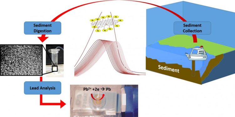
Sediments collected by a ship can be rapidly tested for toxic lead with a new portable lab-on-a-chip device. The miniature device extracts lead from a sample and purifies it, using graphene oxide as a lead detector.
Credit: Azam Gholizadeh
Researchers create portable lab-on-a-chip that could detect many contaminants.
Rutgers researchers have created a miniature device for measuring trace levels of toxic lead in sediments at the bottom of harbors, rivers and other waterways within minutes – far faster than currently available laboratory-based tests, which take days.
The affordable lab-on-a-chip device could also allow municipalities, water companies, universities, K-12 schools, daycares and homeowners to easily and swiftly test their water supplies. The research is published in the IEEE Sensors Journal.
“In addition to detecting lead contamination in environmental samples or water in pipes in homes or elementary schools, with a tool like this, someday you could go to a sushi bar and check whether the fish you ordered has lead or mercury in it,” said senior author Mehdi Javanmard, an associate professor in the Department of Electrical and Computer Engineering in the School of Engineering at Rutgers University-New Brunswick.
“Detecting toxic metals like lead, mercury and copper normally requires collecting samples and sending them to a lab for costly analysis, with results returned in days,” Javanmard said. “Our goal was to bypass this process and build a sensitive, inexpensive device that can easily be carried around and analyze samples on-site within minutes to rapidly identify hot spots of contamination.”
The research focused on analyzing lead in sediment samples. Many river sediments in New Jersey and nationwide are contaminated by industrial and other waste dumped decades ago. Proper management of contaminated dredged materials from navigational channels is important to limit potential impacts on wildlife, agriculture, plants and food supplies. Quick identification of contaminated areas could enable timely and cost-effective programs to manage dredged materials.
The new device extracts lead from a sediment sample and purifies it, with a thin film of graphene oxide as a lead detector. Graphene is an atom thick layer of graphite, the writing material in pencils.
More research is needed to further validate the device’s performance and increase its durability so it can become a viable commercial product, possibly in two to four years.
###
This project was done in collaboration with the Department of Electrical and Computer Engineering and Rutgers’ Center for Advanced Infrastructure and Transportation (CAIT). It was funded by CAIT, the USDOT-University Transportation Research Center-Region II.
The lead author is Azam Gholizadeh, who earned a doctorate at Rutgers. Co-authors include Sakshi Sardar, who also earned a doctorate; Kelly Francisco, a postdoctoral research associate at CAIT; Ali Maher, CAIT director and a professor in the Department of Environmental and Civil Engineering; and Robert Miskewitz, an associate research professor in the Department of Environmental Sciences in the School of Environmental and Biological Sciences.
Original Source
https:/
Related Journal Article
Media Contact
All latest news from the category: Information Technology
Here you can find a summary of innovations in the fields of information and data processing and up-to-date developments on IT equipment and hardware.
This area covers topics such as IT services, IT architectures, IT management and telecommunications.
Newest articles

Magnetic Memory Unlocked with Energy-Efficient MRAM
Researchers from Osaka University introduced an innovative technology to lower power consumption for modern memory devices. Stepping up the Memory Game: Overcoming the Limitations of Traditional RAM Osaka, Japan –…

Next-Level System Security: Smarter Access Control for Organizations
Cutting-Edge Framework for Enhancing System Security Researchers at the University of Electro-Communications have developed a groundbreaking framework for improving system security by analyzing business process logs. This framework focuses on…

How Microbial Life Shapes Lime Formation in the Deep Ocean
Microorganisms are everywhere and have been influencing the Earth’s environment for over 3.5 billion years. Researchers from Germany, Austria and Taiwan have now deciphered the role they play in the…


