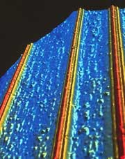
Striped nanowires shrink electronics

Multi-flavoured nanowires can act as miniature bar-codes, diodes and light sources <br>© SPL <br>
Wires one-millionth of a millimetre wide change composition along their length.
Wires one-millionth of a millimetre wide that change chemical composition along their length, just as fruit pastilles change flavour along a packet, have been grown in the United States. These multi-flavoured nanowires can act as miniature bar-codes, diodes and light sources.
Conventional microelectronics components are etched into flat layers of semiconducting material. Charles Lieber and colleagues at Harvard University in Cambridge, Massachusetts, grow their wires – smaller than the thinnest wire on a commercial silicon chip – from vapours of the atomic ingredients.
Lieber’s group perfected their method for making semiconductor nanowires two years ago. They use a tiny blob of a catalyst, which stays at the growing tip of the wire like the point of a pencil tracing out a line. The size of the catalyst particle controls the wire’s width.
Now the researchers report that, by choosing their catalyst carefully – they use gold nanocrystals – they can grow sequential lengths of a single wire from different chemicals1. They use a laser to blast a semiconductor into a vapour, which then condenses into nanowires. Exposing the growing wires first to one kind of vapour and then to another varies the composition along the wire.
Superlattice lines up
The team has made wires about 20 nanometres across that contain alternating sections of the semiconductors gallium arsenide and gallium phosphide. Microelectronic engineers often use structures like this, called superlattices, in electronic devices. They are currently made by carving up flat sandwiches of layered semiconductors.
Superlattices are used, for example, as mirrors in microscopic lasers, or as waveguides to capture and confine light. If electrons are trapped in a thin layer of a semiconductor sandwiched between barriers of a different semiconductor, quantum wells are created that emit light. The colour of the light can be tuned by varying the well thickness.
Nanowire superlattices could be used in all these applications. Their size means that many more could be packed onto a single chip than today’s microelectronics components. The researchers envisage making nanowire lasers, for example.
Up the junction
To demonstrate the wires’ potential, Lieber’s group made structures called p-n junctions. They grew silicon nanowires in two sections, each spiced with a different additive to fine-tune the electrical behaviour of the silicon. These nanowire p-n junctions behave like diodes – they let current flow in only one direction.
The team also made p-n junctions that act as light-emitting diodes. Because these glowing devices are so small, the researchers hope to make them expel light one photon at a time. This could be useful in a new type of ultra-powerful information processing called quantum computing.
References
- Gudiksen, M. S., Lauhon, L. J., Wang, J., Smith, D. C. & Lieber, C. M. Growth of nanowire superlattice structures for nanoscale photonics and electronics. Nature, 415, 617 – 620, (2002).
Media Contact
More Information:
http://www.nature.com/nsu/020204/020204-7.htmlAll latest news from the category: Information Technology
Here you can find a summary of innovations in the fields of information and data processing and up-to-date developments on IT equipment and hardware.
This area covers topics such as IT services, IT architectures, IT management and telecommunications.
Newest articles

First-of-its-kind study uses remote sensing to monitor plastic debris in rivers and lakes
Remote sensing creates a cost-effective solution to monitoring plastic pollution. A first-of-its-kind study from researchers at the University of Minnesota Twin Cities shows how remote sensing can help monitor and…

Laser-based artificial neuron mimics nerve cell functions at lightning speed
With a processing speed a billion times faster than nature, chip-based laser neuron could help advance AI tasks such as pattern recognition and sequence prediction. Researchers have developed a laser-based…

Optimising the processing of plastic waste
Just one look in the yellow bin reveals a colourful jumble of different types of plastic. However, the purer and more uniform plastic waste is, the easier it is to…


