Engineering material magic

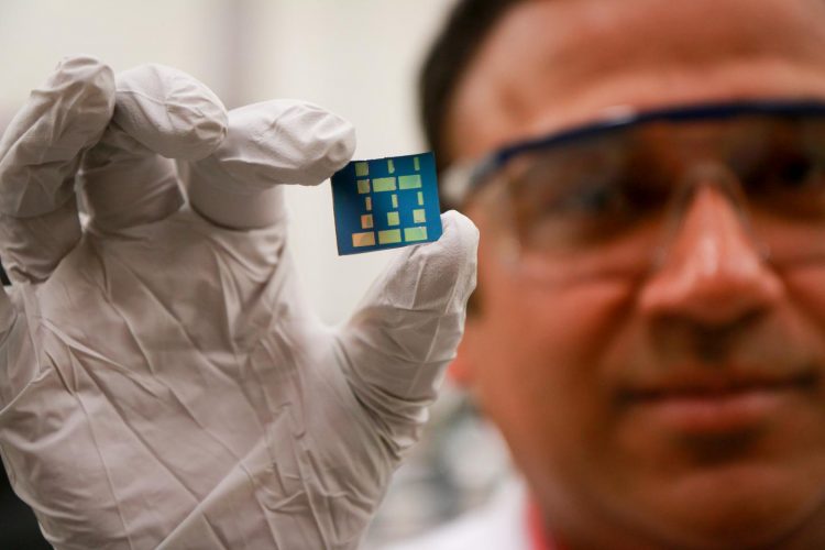
University of Utah materials science and engineering associate professor Ashutosh Tiwari holds up a substrate layered with a newly discovered 2-D material made of tin and oxygen. Tiwari and his team have discovered this new material, tin monoxide, which allows electrical charges to move through it much faster than common 3-D material such as silicon. This breakthrough in semiconductor material could lead to much faster computers and mobile devices such as smartphones that also run on less power and with less heat. Credit: Dan Hixson/University of Utah College of Engineering
University of Utah engineers have discovered a new kind of 2D semiconducting material for electronics that opens the door for much speedier computers and smartphones that also consume a lot less power.
The semiconductor, made of the elements tin and oxygen, or tin monoxide (SnO), is a layer of 2D material only one atom thick, allowing electrical charges to move through it much faster than conventional 3D materials such as silicon.
This material could be used in transistors, the lifeblood of all electronic devices such as computer processors and graphics processors in desktop computers and mobile devices. The material was discovered by a team led by University of Utah materials science and engineering associate professor Ashutosh Tiwari.
A paper describing the research was published online Monday, Feb. 15, 2016 in the journal, Advanced Electronic Materials. The paper, which also will be the cover story on the printed version of the journal, was co-authored by University of Utah materials science and engineering doctoral students K. J. Saji and Kun Tian, and Michael Snure of the Wright-Patterson Air Force Research Lab near Dayton, Ohio.
Transistors and other components used in electronic devices are currently made of 3D materials such as silicon and consist of multiple layers on a glass substrate. But the downside to 3D materials is that electrons bounce around inside the layers in all directions.
The benefit of 2D materials, which is an exciting new research field that has opened up only about five years ago, is that the material is made of one layer the thickness of just one or two atoms. Consequently, the electrons “can only move in one layer so it's much faster,” says Tiwari.
While researchers in this field have recently discovered new types of 2D material such as graphene, molybdenun disulfide and borophene, they have been materials that only allow the movement of N-type, or negative, electrons. In order to create an electronic device, however, you need semiconductor material that allows the movement of both negative electrons and positive charges known as “holes.” The tin monoxide material discovered by Tiwari and his team is the first stable P-type 2D semiconductor material ever in existence.
“Now we have everything — we have P-type 2D semiconductors and N-type 2D semiconductors,” he says. “Now things will move forward much more quickly.”
Now that Tiwari and his team have discovered this new 2D material, it can lead to the manufacturing of transistors that are even smaller and faster than those in use today. A computer processor is comprised of billions of transistors, and the more transistors packed into a single chip, the more powerful the processor can become.
Transistors made with Tiwari's semiconducting material could lead to computers and smartphones that are more than 100 times faster than regular devices. And because the electrons move through one layer instead of bouncing around in a 3D material, there will be less friction, meaning the processors will not get as hot as normal computer chips. They also will require much less power to run, a boon for mobile electronics that have to run on battery power. Tiwari says this could be especially important for medical devices such as electronic implants that will run longer on a single battery charge.
“The field is very hot right now, and people are very interested in it,” Tiwari says. “So in two or three years we should see at least some prototype device.”
Media Contact
All latest news from the category: Materials Sciences
Materials management deals with the research, development, manufacturing and processing of raw and industrial materials. Key aspects here are biological and medical issues, which play an increasingly important role in this field.
innovations-report offers in-depth articles related to the development and application of materials and the structure and properties of new materials.
Newest articles

Innovative vortex beam technology
…unleashes ultra-secure, high-capacity data transmission. Scientists have developed a breakthrough optical technology that could dramatically enhance the capacity and security of data transmission (Fig. 1). By utilizing a new type…

Tiny dancers: Scientists synchronise bacterial motion
Researchers at TU Delft have discovered that E. coli bacteria can synchronise their movements, creating order in seemingly random biological systems. By trapping individual bacteria in micro-engineered circular cavities and…

Primary investigation on ram-rotor detonation engine
Detonation is a supersonic combustion wave, characterized by a shock wave driven by the energy release from closely coupled chemical reactions. It is a typical form of pressure gain combustion,…


