Large-scale field-effect transistors based on solution-grown organic single crystals are fabricated

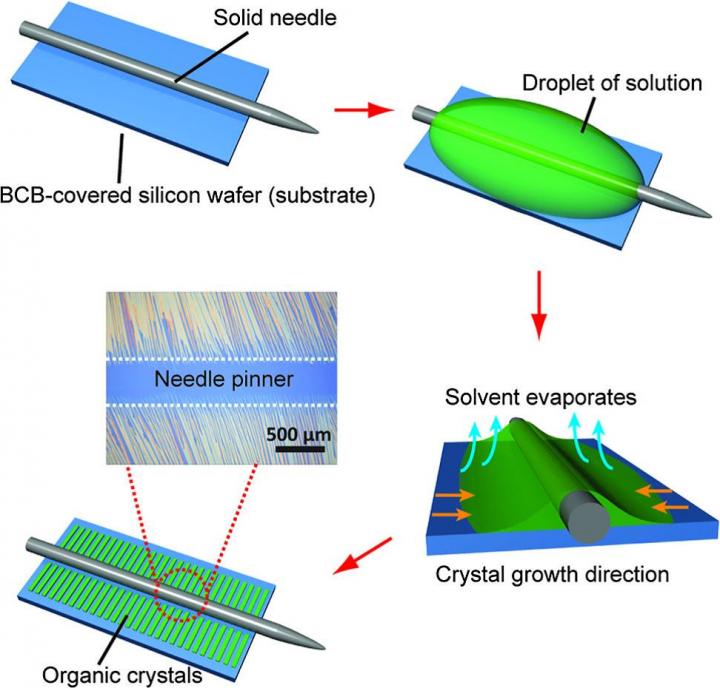
This image shows an experimental procedure to achieve crystal alignment. Credit: ©Science China Press
However, single-crystal devices are practically difficult to fabricate. For both fundamental studies and technological applications, high-throughput fabrication of single-crystal FETs is highly desired for either examination of device performance statistics or realization of a large array of devices and has attracted the attention of researchers from both academia and industry.
In an article published in Science Bulletin, Prof. Hanying Li's research group describe a simple solution processing method where well-aligned single-crystals of organic semiconductors throughout a 1cm × 2cm substrate can be grown from a droplet pinned by a metal needle.
The well-controlled alignment of the crystals originates from the unidirectional receding of the pinned droplet regulated by the capillary force. Because of the crystal alignment in a large area, fabrication of device arrays become possible.
More importantly, this simple method is applicable to a wide range of organic semiconductors and potentially to inorganic materials, with six examples including both p- and n-channel materials demonstrated in this work.
Furthermore, large-scale FET arrays are fabricated and studied, using TIPS-pentacene crystals (a well-known p-channel material) as an example.
Among the 330 devices randomly selected from 2 substrates, an average hole mobility (μ) of 3.44 ± 1.21 cm2V-1s-1 with the maximum value of 6.46 cm2V-1s-1, on-to-off current ratios (I on/I off) > 10 5, and threshold voltages (VT) between -20 to -58 V were achieved.
Among the 330 devices, 328 FETs showed the mobility above 1 cm2V-1s-1, the other two were 0.94 cm2V-1s-1 and 0.92 cm2V-1s-1 respectively. The achieved FET performance is among the best reported ones. As such, this work provides a highly efficient, yet simple approach to evaluate the charge transport properties of organic semiconductors through examining the performance statistics of single-crystal devices.
###
See the article:
Shuang Liu, Jiake Wu, Congcheng Fan, Guobiao Xue, Hongzheng Chen, Huolin L. Xin and Hanying Li, “Large-scale fabrication of field-effect transistors based on solution-grown organic single crystals,” Science Bulletin, 2015, 60(12): 1122-1127. doi: 10.1007/s11434-015-0817-9.
http://www.
http://link.
Media Contact
All latest news from the category: Materials Sciences
Materials management deals with the research, development, manufacturing and processing of raw and industrial materials. Key aspects here are biological and medical issues, which play an increasingly important role in this field.
innovations-report offers in-depth articles related to the development and application of materials and the structure and properties of new materials.
Newest articles

First-of-its-kind study uses remote sensing to monitor plastic debris in rivers and lakes
Remote sensing creates a cost-effective solution to monitoring plastic pollution. A first-of-its-kind study from researchers at the University of Minnesota Twin Cities shows how remote sensing can help monitor and…

Laser-based artificial neuron mimics nerve cell functions at lightning speed
With a processing speed a billion times faster than nature, chip-based laser neuron could help advance AI tasks such as pattern recognition and sequence prediction. Researchers have developed a laser-based…

Optimising the processing of plastic waste
Just one look in the yellow bin reveals a colourful jumble of different types of plastic. However, the purer and more uniform plastic waste is, the easier it is to…


