Manipulation of the characteristics of magnetic materials

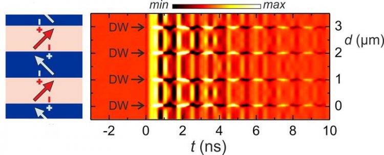
In the simulation, magnetic signals spread along the domain walls in a few nanoseconds. The signals behave in a wave-like manner, with the initially high amplitude rapidly becoming smaller. McCord
Splitting a magnetic material into small domains has significant energy benefits. But the focus of the research team from Kiel University is on the walls which separate the domains from each other.
“The position and the density of these walls determine the characteristics of the entire magnetic layer,” said Jeffrey McCord, Professor of Nanoscale Magnetic Materials, with a focus on magnetic domains. “Being able to specifically set the positions of domain walls, therefore, has a major impact – but it's not all that easy to do,” said the leader of the research team.
In order to precisely position the domains and domain walls, the research team used a special method: the scientists irradiated magnetic multilayer films with ions. Domain wall structures, which are normally arranged randomly, can thereby be “imprinted” in the magnetic material as desired.
“In this way, magnetic characteristics can be specifically modified, and on a reproducible basis as well. We can thus determine the positions of the domain walls ourselves and build our own domain wall gratings out of millions of 50-nanometre-wide walls. This allows us to create magnetic materials which display a completely different behaviour to external magnetic fields,” said a delighted McCord.
“We were surprised at how well spin waves spread in the domain walls and are directed by them,” emphasised McCord. Electron spins are also suitable for processing and encoding information.
In the long term, therefore, the discoveries made by the Kiel scientists could be interesting for data transfer that does not take place via electrons, but via magnons – i.e. magnetic information transfer. “With artificially created domain wall structures, we can direct data streams faster and with less energy,” said McCord. Further areas of application include highly-sensitive magnetic sensors.
Original publication:
J. Trützschler, K. Sentosun, B. Mozooni, R. Mattheis, J. McCord. Magnetic domain wall gratings for magnetization reversal tuning and confined dynamic mode localization, Scientific Reports 6, 30761 (2016) DOI: 10.1038/srep30761
www.nature.com/articles/srep30761
Photos are available to download:
www.uni-kiel.de/download/pm/2016/2016-387-1.jpg
In the simulation, magnetic signals spread along the domain walls (DW) in a few nanoseconds (ns). In ten nanoseconds, a ray of light travels three metres. The signals behave in a wave-like manner, with the initially high amplitude rapidly becoming smaller.
Photo/Copyright: McCord
www.uni-kiel.de/download/pm/2016/2016-387-2.jpg
Jeffrey McCord has been working as Professor for Nanoscale Magnetic Materials, focusing on magnetic domains, at Kiel University since 2011.
Photo/Copyright: Denis Schimmelpfennig / Kiel University
Contact:
Jeffrey McCord
Institute for Materials Science
Professor for Nanoscale Magnetic Materials
Tel.: +49 (0)431 880 6123
E-mail: jemc@tf.uni-kiel.de
Details, which are only a millionth of a millimetre in size: This is what the research focus “Kiel Nano, Surface and Interface Science – KiNSIS” at Kiel University has been working on. In the nano-cosmos, different laws prevail than in the macroscopic world – those of quantum physics. Through intensive, interdisciplinary cooperation between materials science, chemistry, physics, biology, electrical engineering, computer science, food technology and various branches of medicine, the research focus aims to understand the systems in this dimension and to implement the findings in an application-oriented manner. Molecular machines, innovative sensors, bionic materials, quantum computers, advanced therapies and much more could be the result. More information at www.kinsis.uni-kiel.de
Kiel University
Press, Communication and Marketing, Dr Boris Pawlowski, Text: Julia Siekmann
Postal address: D-24098 Kiel, Germany,
Telephone: +49 (0)431 880-2104, Fax: +49 (0)431 880-1355
E-mail: presse@uv.uni-kiel.de, Internet: www.uni-kiel.de
Twitter: www.twitter.com/kieluni, Facebook: www.facebook.com/kieluni
Media Contact
All latest news from the category: Materials Sciences
Materials management deals with the research, development, manufacturing and processing of raw and industrial materials. Key aspects here are biological and medical issues, which play an increasingly important role in this field.
innovations-report offers in-depth articles related to the development and application of materials and the structure and properties of new materials.
Newest articles

Compact LCOS Microdisplay with Fast CMOS Backplane
…for High-Speed Light Modulation. Researchers from the Fraunhofer Institute for Photonic Microsystems IPMS, in collaboration with HOLOEYE Photonics AG, have developed a compact LCOS microdisplay with high refresh rates that…

New perspectives for material detection
CRC MARIE enters third funding period: A major success for terahertz research: Scientists at the University of Duisburg-Essen and the Ruhr University Bochum have been researching mobile material detection since…

CD Laboratory at TU Graz Researches New Semiconductor Materials
Using energy- and resource-saving methods, a research team at the Institute of Inorganic Chemistry at TU Graz aims to produce high-quality doped silicon layers for the electronics and solar industries….


