Mapping the defects of a supermaterial

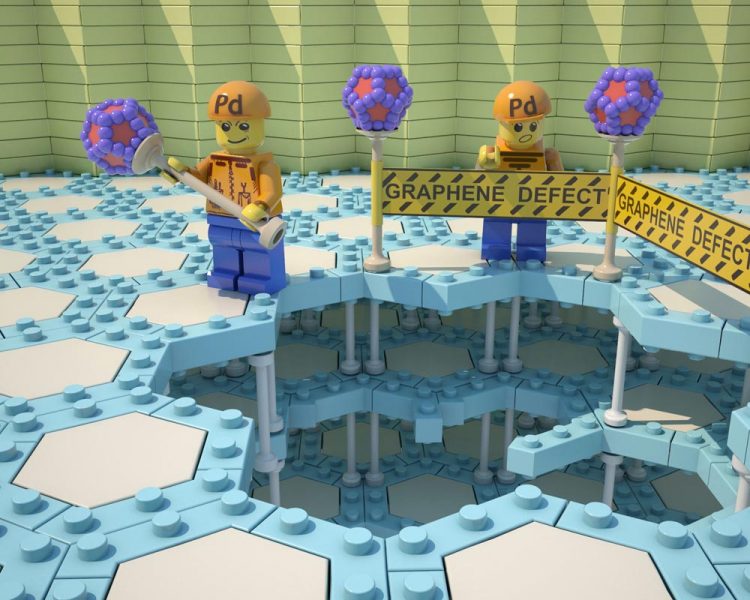
Artistic image on the concept of imaging of carbon defect areas by palladium markers. (Graphene defects marked by Pd). Copyright : Ananikov Laboratory, Zelinsky Institute of Organic Chemistry
The technique, developed by researchers at the Zelinsky Institute of Organic Chemistry in a collaborative project, employs the metal palladium, which interacts with “carbon reactivity centres” found on graphene. Graphene is an incredibly strong one-atom-thick layer of carbon touted to be an excellent conductor of heat and electricity.
Several types of defects on graphene surfaces are known to increase the reactivity of its carbon atoms: i.e. their ability to form chemical bonds. If researchers can locate these defects and manipulate them, they will be able to maximize the use of graphene’s properties.
For example, locating and removing defects is important for applications that require perfectly smooth graphene. In other applications, such as in catalysis and certain biomedical materials, some defects are actually beneficial because they allow the incorporation of additional elements, such as metals, into the graphene.
When the palladium complex Pd2(dba)3 is dissolved in chloroform, it forms a dark red solution under normal circumstances. But when graphene or another carbon material is added to the solution, the palladium is completely consumed. As a result, the solution turns from dark red to colourless.
Using advanced imaging techniques, the researchers found that the palladium clusters selectively attach to graphene’s surface according to specific patterns, depending on how reactive the carbon centres are. Individual palladium particles settle onto point defects, local accumulations of particles are present on larger defects, and short chains outline linear defects.
These defects are normally invisible under an electron microscope. The palladium particles act like a contrast agent, allowing the spatial imaging of the chemical reactivity, and thus the defects, of graphene layers.
“Metal mapping of carbon materials provides unique insights and reveals hidden information about fascinating properties at the molecular level,” says project leader Professor Valentine Ananikov.
The team’s findings indicate that using palladium markers, more than 2,000 surface defects, or reactivity centres, on graphene can be individually located, per square micrometre of surface area. The researchers say that the unexpected capacity of graphene to accommodate so many reactivity centres challenges scientists to re-examine their understanding of the electronic and structural properties of carbon materials.
Now that the researchers have learned how to recognise and characterise the defects, their next step is to develop a technique to control them. Some defects possess a dynamic nature and have the ability to “migrate” over graphene’s surface. If the researchers can control this migration, they will have a unique opportunity to form materials with customised properties. This is an outstanding direction for future studies, they say.
For further information contact:
Professor Valentine P. Ananikov
Zelinsky Institute of Organic Chemistry
Moscow, Russia
E-mail: val@ioc.ac.ru
Associated links
Media Contact
All latest news from the category: Materials Sciences
Materials management deals with the research, development, manufacturing and processing of raw and industrial materials. Key aspects here are biological and medical issues, which play an increasingly important role in this field.
innovations-report offers in-depth articles related to the development and application of materials and the structure and properties of new materials.
Newest articles

First-of-its-kind study uses remote sensing to monitor plastic debris in rivers and lakes
Remote sensing creates a cost-effective solution to monitoring plastic pollution. A first-of-its-kind study from researchers at the University of Minnesota Twin Cities shows how remote sensing can help monitor and…

Laser-based artificial neuron mimics nerve cell functions at lightning speed
With a processing speed a billion times faster than nature, chip-based laser neuron could help advance AI tasks such as pattern recognition and sequence prediction. Researchers have developed a laser-based…

Optimising the processing of plastic waste
Just one look in the yellow bin reveals a colourful jumble of different types of plastic. However, the purer and more uniform plastic waste is, the easier it is to…


