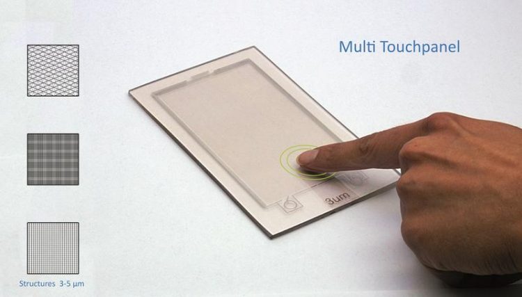
Novel process allows production of the entire circuitry on touchscreens in one step

Electronic micro and conductor strips via Photometallization. Source: INM; free within this press release
All that concerns them is that they can happily swipe and tap away. To make the touchscreens work, they are provided on their surface with microscopically small electrical conductor tracks, which open and close circuits when touched with a finger. At the peripheries of the devices, these microscopic tracks merge into larger conductor tracks.The researchers at the INM – Leibniz-Institute for New Materials are now presenting a novel process that allows microscopic and macroscopic conductor tracks to be produced in one step.
The INM from Saarbruecken will be one of the few German research institutions at the TechConnect World trade fair on 16 and 17 June in Washington DC, USA, where it will be presenting this and other results. Working in cooperation with the VDI Association of German Engineers it will be showcasing its latest developments at Stand 301 in the German Area.
The developers are basing the novel process on photometallization: under exposure to UV light, and acting in conjunction with a photoactive layer, colourless silver compounds turn into electrically conductive silver. The silver compound can be applied in the form of tracks or other structures to plastic films or glass by various methods. Tracks of various sizes, down to the smallest size of a 1000th of a millimetre, can be created in this way. The corresponding conductor tracks are then produced by exposure to UV light.
The films or glass are first coated with a photoactive layer of metal oxide nanoparticles. “We then apply the colourless, UV-stable silver compound”, says Peter William de Oliveira, Head of the Optical Materials Program Division. The exposure of this series of layers has the effect that the silver compound on the photoactive layer decomposes and the silver ions are reduced to metallic, electrically conductive silver. This process is said to have several advantages: it is claimed to be quick, flexible, variable in scale, low in cost and environmentally friendly. And there is no need for any further post-treatment process steps.
This basic principle allows researchers at the INM to very individually apply conductor strips of different sizes to substrates such as glass or plastic. “There are three different options that we can use as required. “Writing” using a UV laser is particularly good for the first customized production and testing of a new conductor strip design, but this method is too time-consuming for mass production”, explains physicist de Oliveira.
Photomasks that are only UV-permeable at the desired positions can also be used for structuring. “The production of these masks is quite costly and has a high environmental impact. For a “semi-continuous process” they are particularly suitable for solid substrates such as glass”, says the materials expert, but they were not suitable for a potential roll-to-roll process because they are mainly composed of quartz glass and are not flexible.
The researchers are currently focusing their efforts on a third method using so-called transparent stamps. “These stamps mechanically displace the silver complex, and where there is no silver there is also no conductor strip”, in de Oliveira’s opinion. “So we can form structures measuring just a few micrometers. Since the stamps are made of a flexible polymer, we have here the possibility of arranging them on a roll. Because they are transparent, we are working on incorporating the UV source in the roll, so the first steps would be done for a roll-to-roll process”, the Head of the Program Division sums up. This has enabled conductor strip structures of different sizes to be produced on substrates such as polyethylene or polycarbonate film on a large scale.
Your expert:
Dr. Peter William de Oliveira
INM – Leibniz Institute for New Materials
Head Optical Materials
Phone: +49681-9300-148
peter.oliveira@inm-gmbh.de
INM conducts research and development to create new materials – for today, tomorrow and beyond. Chemists, physicists, biologists, materials scientists and engineers team up to focus on these essential questions: Which material properties are new, how can they be investigated and how can they be tailored for industrial applications in the future? Four research thrusts determine the current developments at INM: New materials for energy application, new concepts for medical surfaces, new surface materials for tribological applications and nano safety and nano bio. Research at INM is performed in three fields: Nanocomposite Technology, Interface Materials, and Bio Interfaces.
INM – Leibniz Institute for New Materials, situated in Saarbruecken, is an internationally leading centre for materials research. It is an institute of the Leibniz Association and has about 195 employees.
Media Contact
More Information:
http://www.inm-gmbh.deAll latest news from the category: Materials Sciences
Materials management deals with the research, development, manufacturing and processing of raw and industrial materials. Key aspects here are biological and medical issues, which play an increasingly important role in this field.
innovations-report offers in-depth articles related to the development and application of materials and the structure and properties of new materials.
Newest articles

First-of-its-kind study uses remote sensing to monitor plastic debris in rivers and lakes
Remote sensing creates a cost-effective solution to monitoring plastic pollution. A first-of-its-kind study from researchers at the University of Minnesota Twin Cities shows how remote sensing can help monitor and…

Laser-based artificial neuron mimics nerve cell functions at lightning speed
With a processing speed a billion times faster than nature, chip-based laser neuron could help advance AI tasks such as pattern recognition and sequence prediction. Researchers have developed a laser-based…

Optimising the processing of plastic waste
Just one look in the yellow bin reveals a colourful jumble of different types of plastic. However, the purer and more uniform plastic waste is, the easier it is to…


