Graphene and other single-atom-thick substances are a category of wonder materials, with researchers the world over investigating their electronic properties for potential applications in technologies as diverse as solar cells, novel semiconductors, sensors, and energy storage.
The greatest challenge for the design of these single-layer or 2D materials into all their myriad potential uses is the need for an atom-by-atom perfection and uniformity that can be difficult and painstaking to achieve at such small scales, and difficult to assess as well.
“We are trying to be more clever than nature in assembling these materials,” said Michael C. Tringides, a senior scientist at the U.S. Department of Energy’s Ames Laboratory and professor of physics at Iowa State University, who investigates the unique properties of 2D materials and metals grown on graphene, graphite, and other carbon coated surfaces. “And to do so, we’re forcing atoms to assemble in ways they normally would not. One of the major challenges of the field is to reliably produce high quality graphene and other materials like it.”
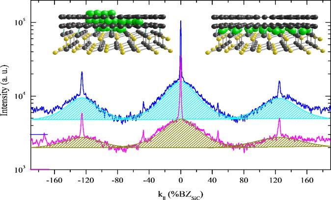
Tringides and other scientists at Ames Laboratory have discovered and confirmed a method which could serve as an easy but reliable way to test the quality of graphene and other 2D materials. It takes advantage of the very broad background in surface electron diffraction, named the Bell-Shaped-Component (BSC) which strongly correlates to uniformly patterned, or “perfect” graphene.
Understanding the correlation has implications for reliable quality control of 2D materials in a manufacturing environment.
“This discovery challenges conventional wisdom, but the correlation between this strange phenomenon and high quality graphene is unmistakable. In practical application, we see it extending to other high-interest 2D materials that are similar to graphene in having similar uniformity of a single layer,” said Tringides.
Last year, Ames Laboratory researchers discovered through low energy electron diffraction– a technique commonly used in physics to study the crystal structure of the surfaces of solid materials– that broad diffraction patterns are an indicator that reliably demonstrates a 2D material’s high quality. It was a feature of high quality graphene that essentially lurked in the background, and had been overlooked in published research because it was the exact opposite of what is generally accepted from diffraction studies–that only sharp, bright diffraction spots should be present. Because that finding was counterintuitive, further investigation was required under different experimental conditions and to understand the origin of the BSC, said Tringides.
First, the scientists grew graphene by annealing, or heating it, through a range of high temperatures, and comparing the growth of the BSC diffraction along with the growth of the other, generally accepted indicator of sharp diffraction spots. The evolution of the broad diffraction background closely mirrored that of the sharper spot, which proved that they are correlated. Secondly, the group then experimented with depositing metal atoms (in this case dysprosium) on the surface and underneath the graphene. Called intercalation, this deposition process is one of the ways scientists can customize 2D materials for specific functions. In the second experiment, scientists measured the growth of the BSC during intercalation– weak when the metal atoms are at first disordered, and then increasing as the metal atoms snap into place between the graphene and the substrate, creating a uniform layer. So while the BSC was not a textbook diffraction pattern, its cause is textbook quantum mechanics– as electrons are squeezed into a single layer, their wave vectors must spread, creating the broad diffraction pattern.
###
The research is further discussed in the paper “High Layer Uniformity of Two-Dimensional Materials Demonstrated Surprisingly from Broad Features in Surface Electron Di?raction,” authored by S. Chen, M. Horn von Hoegen, P. A. Thiel, A. Kaminski, B. Schrunk, T. Speliotis, E. H. Conrad, and M. C. Tringides; and published in the Journal of Physical Chemistry Letters.
Ames Laboratory is a U.S. Department of Energy Office of Science National Laboratory operated by Iowa State University. Ames Laboratory creates innovative materials, technologies and energy solutions. We use our expertise, unique capabilities and interdisciplinary collaborations to solve global problems.
Ames Laboratory is supported by the Office of Science of the U.S. Department of Energy. The Office of Science is the single largest supporter of basic research in the physical sciences in the United States, and is working to address some of the most pressing challenges of our time. For more information, please visit https:/
Original Source https:/


