Replacement for silicon devices looms big with ORNL discovery

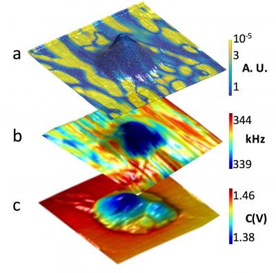
This diagram illustrates the effect of helium ions on the mechanical and electrical properties of the layered ferroelectric: a.) Disappearance domains in the exposed area; as the mound forms yellow regions (ferroelectricity) gradually disappear; b.) Mechanical properties of the material; warmer colors indicate hard areas, cool colors indicate soft areas; c.) Conductivity enhancement; warmer colors show insulating areas, cooler colors show more conductive areas. Credit: ORNL
A team led by Olga Ovchinnikova of ORNL's Center for Nanophase Materials Sciences Division used a helium ion microscope, an atomic-scale “sandblaster,” on a layered ferroelectric surface of a bulk copper indium thiophosphate. The result, detailed in the journal ACS Applied Materials and Interfaces, is a surprising discovery of a material with tailored properties potentially useful for phones, photovoltaics, flexible electronics and screens.
“Our method opens pathways to direct-write and edit circuitry on 2-D material without the complicated current state-of-the-art multi-step lithographic processes,” Ovchinnikova said.
She and colleague Alex Belianinov noted that while the helium ion microscope is typically used to cut and shape matter, they demonstrated that it can also be used to control ferroelectric domain distribution, enhance conductivity and grow nanostructures. Their work could establish a path to replace silicon as the choice for semiconductors in some applications.
“Everyone is looking for the next material – the thing that will replace silicon for transistors,” said Belianinov, the lead author. “2-D devices stand out as having low power consumption and being easier and less expensive to fabricate without requiring harsh chemicals that are potentially harmful to the environment.”
Reducing power consumption by using 2-D-based devices could be as significant as improving battery performance. “Imagine having a phone that you don't have to recharge but once a month,” Ovchinnikova said.
###
The paper, titled “Polarization control via He-ion beam induced nanofabrication in layered ferroelectric semiconductors,” is available at http://pubs.
This research was funded through the Laboratory Directed Research and Development program. Some of the work was performed at the Center for Nanophase Materials Sciences, a DOE Office of Science User Facility.
UT-Battelle manages ORNL for the DOE's Office of Science. The Office of Science is the single largest supporter of basic research in the physical sciences in the United States, and is working to address some of the most pressing challenges of our time. For more information, please visit http://science.
Image: https:/
Cutline: This diagram illustrates the effect of helium ions on the mechanical and electrical properties of the layered ferroelectric: a.) Disappearance domains in the exposed area; as the mound forms yellow regions (ferroelectricity) gradually disappear; b.) Mechanical properties of the material; warmer colors indicate hard areas, cool colors indicate soft areas; c.) Conductivity enhancement; warmer colors show insulating areas, cooler colors show more conductive areas.
NOTE TO EDITORS: You may read other press releases from Oak Ridge National Laboratory or learn more about the lab at http://www.
Twitter – http://twitter.
RSS Feeds – http://www.
Flickr – http://www.
YouTube – http://www.
LinkedIn – http://www.
Facebook – http://www.
Media Contact
All latest news from the category: Materials Sciences
Materials management deals with the research, development, manufacturing and processing of raw and industrial materials. Key aspects here are biological and medical issues, which play an increasingly important role in this field.
innovations-report offers in-depth articles related to the development and application of materials and the structure and properties of new materials.
Newest articles

First-of-its-kind study uses remote sensing to monitor plastic debris in rivers and lakes
Remote sensing creates a cost-effective solution to monitoring plastic pollution. A first-of-its-kind study from researchers at the University of Minnesota Twin Cities shows how remote sensing can help monitor and…

Laser-based artificial neuron mimics nerve cell functions at lightning speed
With a processing speed a billion times faster than nature, chip-based laser neuron could help advance AI tasks such as pattern recognition and sequence prediction. Researchers have developed a laser-based…

Optimising the processing of plastic waste
Just one look in the yellow bin reveals a colourful jumble of different types of plastic. However, the purer and more uniform plastic waste is, the easier it is to…


