Precision bonding makes tiny high performance actuators possible

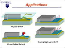
Some possible applications of the new Penn State piezoelectric microactuator
Using a new precision bonding process they developed, Penn State researchers have designed and fabricated tiny new piezoelectric microactuators — the largest only a hair’s breadth wide — based on coupling commercially available materials with existing micromachining technology.
The new actuators promise to be low cost, and capable of providing controlled force, high resolution and large displacements appropriate for applications in RF switches for cell phones, for example, or optical switches for wide screen TVs. Other potential applications include microfluidic pumps and valves, micromanipulators for nanoscale handling and atomic force microscope drives.
Dr. Srinivas A. Tadigadapa, associate professor of electrical engineering and a developer of the bonding process and microactuator, says, “These new piezoelectric microactuators are the first realized using microfabrication methods, a mature technology used to make computer chips and micromachines from silicon-based materials. Our new low temperature wafer bonding techniques, which make the actuators possible, can also be used for precision integration of dissimilar materials in other micro-electro-mechanical systems.”
The new actuators and bonding process are described in a paper, Fabrication and performance of a flextensional microactuator, which appears in the current online edition of the Journal of Micromechanics and Microengineering (JMM). The paper will also be featured in the October print version of JMM.
The authors are Jongpil Cheong, who earned his doctorate at Penn State this year, Abhijat Goyal, a doctoral candidate in electrical engineering, Dr. Tadigadapa and Dr. Christopher D. Rahn, professor of mechanical engineering.
The new actuators are made from flat strips of bulk PZT, a commercially available piezoelectric material that shrinks slightly when a voltage is applied to it, and a precision micromachined silicon beam. Bonding the silicon beam to the PZT amplifies and converts the PZT shape change into a convex deflection when the silicon beam buckles as the PZT shrinks.
In operation in the actuator, the measured deflection of the silicon beam shows a gain factor of 20 with respect to the PZT dimensional change.
For the bonding process in fabricating the new actuators, the Penn State researchers use photolithography and low temperature solders to produce the distinctive bridge shape they need.
Dr. Tadigadapa notes, “The PZT depoles if you heat it too high. Therefore, the temperature is crucial. A low temperature solder bonding process at 200 C was used in this work.”
Using their new approach, the researchers have fabricated actuators with dimensions ranging from 350 to 600 microns in length, 50 to 100 microns (about the width of a human hair) in width, and 5 to 6 microns in thickness.
In tests, the actuators showed good repeatability with a large amplitude stroke of about 8 microns when actuated using -100V to 100V. The bandwidth of the actuator was measured at 265 KHz.
Media Contact
More Information:
http://www.psu.eduAll latest news from the category: Materials Sciences
Materials management deals with the research, development, manufacturing and processing of raw and industrial materials. Key aspects here are biological and medical issues, which play an increasingly important role in this field.
innovations-report offers in-depth articles related to the development and application of materials and the structure and properties of new materials.
Newest articles

First-of-its-kind study uses remote sensing to monitor plastic debris in rivers and lakes
Remote sensing creates a cost-effective solution to monitoring plastic pollution. A first-of-its-kind study from researchers at the University of Minnesota Twin Cities shows how remote sensing can help monitor and…

Laser-based artificial neuron mimics nerve cell functions at lightning speed
With a processing speed a billion times faster than nature, chip-based laser neuron could help advance AI tasks such as pattern recognition and sequence prediction. Researchers have developed a laser-based…

Optimising the processing of plastic waste
Just one look in the yellow bin reveals a colourful jumble of different types of plastic. However, the purer and more uniform plastic waste is, the easier it is to…


