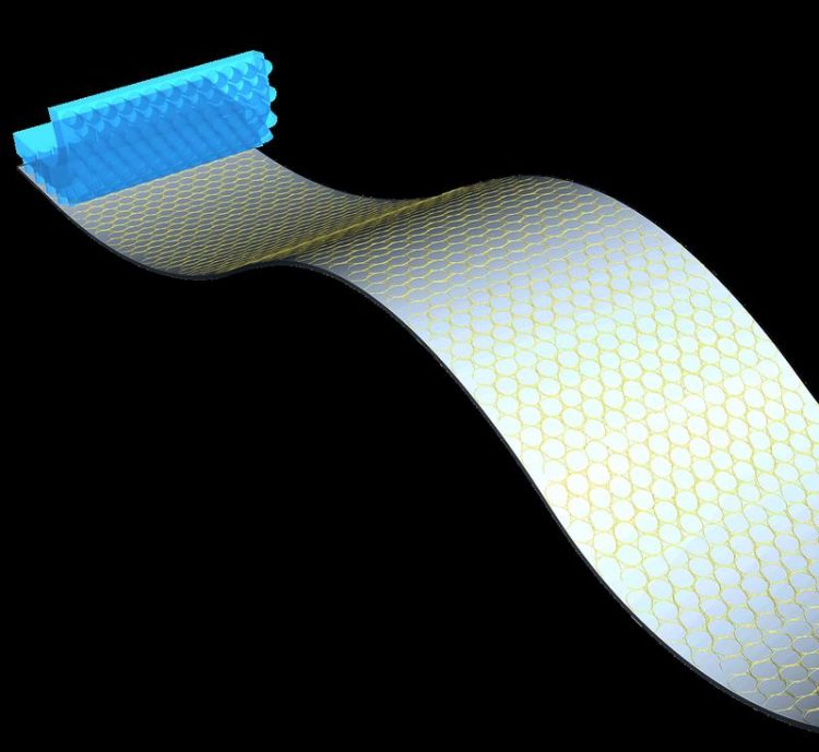
Self-assembling nano inks form conductive and transparent grids during imprint

Self-assembling nano inks form conductive and transparent grids during imprint. Copyright: INM
To print the grids, an ink of gold nanowires is applied to a substrate. A structured stamp is pressed on the substrate and forces the ink into a pattern. “The nanowires are extremely thin and flexible; they adapt to any pattern of the stamp. During drying, the individual wires self-assemble and form larger, percolating bundles that form the grid,” explains Tobias Kraus from INM.
The stamp is removed and the grid is treated in a plasma. “This compresses the bundles into conductive wires and results in a transparent, conductive grid. Depending on the geometry of the stamp, this simple method can shape any nano or microgrid,” says Kraus, head of the program division Structure Formation.
The thickness of the grid can be controlled via the gold concentration. “Only very small quantities of gold are needed to produce a conductive grid, far less than when using inks with spherical gold particles,” says Kraus. This makes the advantages of gold accessible for flexible electronics.
“Our results show self-assembly and imprint can be combined to efficiently produce transparent, conductive materials. We will transfer this insight to other metals in further studies,” says Kraus.
Further information can be found in the original publication:
Maurer, Johannes H. M., González-García, Lola, Reiser, Beate, Kanelidis, Ioannis, Kraus, Tobias, Templated self-assembly of ultrathin gold nanowires by nanoimprinting for transparent flexible electronics, Nano Letters, http://dx.doi.org/10.1021/acs.nanolett.5b04319
Your expert:
Dr. Tobias Kraus
INM – Leibniz Institute for New Materials
Head Structure Formation
Deputy Head InnovationCenter INM
Phone: +49681-9300-389
tobias.kraus@leibniz-inm.de
INM conducts research and development to create new materials – for today, tomorrow and beyond. Chemists, physicists, biologists, materials scientists and engineers team up to focus on these essential questions: Which material properties are new, how can they be investigated and how can they be tailored for industrial applications in the future? Four research thrusts determine the current developments at INM: New materials for energy application, new concepts for medical surfaces, new surface materials for tribological systems and nano safety and nano bio. Research at INM is performed in three fields: Nanocomposite Technology, Interface Materials, and Bio Interfaces.
INM – Leibniz Institute for New Materials, situated in Saarbrücken, is an internationally leading centre for materials research. It is an institute of the Leibniz Association and has about 220 employees.
Media Contact
All latest news from the category: Materials Sciences
Materials management deals with the research, development, manufacturing and processing of raw and industrial materials. Key aspects here are biological and medical issues, which play an increasingly important role in this field.
innovations-report offers in-depth articles related to the development and application of materials and the structure and properties of new materials.
Newest articles

First-of-its-kind study uses remote sensing to monitor plastic debris in rivers and lakes
Remote sensing creates a cost-effective solution to monitoring plastic pollution. A first-of-its-kind study from researchers at the University of Minnesota Twin Cities shows how remote sensing can help monitor and…

Laser-based artificial neuron mimics nerve cell functions at lightning speed
With a processing speed a billion times faster than nature, chip-based laser neuron could help advance AI tasks such as pattern recognition and sequence prediction. Researchers have developed a laser-based…

Optimising the processing of plastic waste
Just one look in the yellow bin reveals a colourful jumble of different types of plastic. However, the purer and more uniform plastic waste is, the easier it is to…


