Semiconductor Works Better When Hitched to Graphene

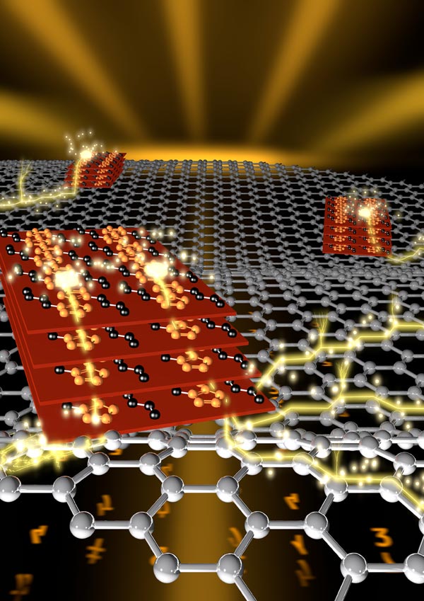
David Barbero A material made of semiconducting polymer placed on top of graphene conducts electric charge extremely well and may enable new electronic devices. This work was featured on the cover of the journal Advanced Functional Materials.
Graphene – a one-atom-thick sheet of carbon with highly desirable electrical properties, flexibility and strength – shows great promise for future electronics, advanced solar cells, protective coatings and other uses, and combining it with other materials could extend its range even further.
Experiments at the Department of Energy’s SLAC National Accelerator Laboratory looked at the properties of materials that combine graphene with a common type of semiconducting polymer. They found that a thin film of the polymer transported electric charge even better when grown on a single layer of graphene than it does when placed on a thin layer of silicon.
“Our results are among the first to measure the charge transport in these materials in the vertical direction – the direction that charge travels in organic photovoltaic devices like solar cells or in light-emitting diodes,” said David Barbero of Umeå University in Sweden, leader of the international research team that performed the experiments at SLAC’s Stanford Synchrotron Radiation Lightsource (SSRL), a DOE Office of Science User Facility. “The result was somewhat expected, because graphene and silicon have different crystalline structures and electrical properties.”
But the team also discovered something very unexpected, he said.
Although it was widely believed that a thinner polymer film should enable electrons to travel faster and more efficiently than a thicker film, Barbero and his team discovered that a polymer film about 50 nanometers thick conducted charge about 50 times better when deposited on graphene than the same film about 10 nanometers thick.
The team concluded that the thicker film’s structure, which consists of a mosaic of crystallites oriented at different angles, likely forms a continuous pathway of interconnected crystals. This, they theorize, allows for easier charge transport than in a regular thin film, whose thin, plate-like crystal structures are oriented parallel to the graphene layer.
By better controlling the thickness and crystalline structure of the semiconducting film, it may be possible to design even more efficient graphene-based organic electronic devices.
“The fields most likely to benefit from this work are probably next-generation photovoltaic devices and flexible electronic devices,” said Barbero. “Because graphene is thin, lightweight and flexible, there are a number of potential applications.”
SLAC is a multi-program laboratory exploring frontier questions in photon science, astrophysics, particle physics and accelerator research. Located in Menlo Park, Calif., SLAC is operated by Stanford University for the U.S. Department of Energy's Office of Science. For more information, please visit slac.stanford.edu
SLAC National Accelerator Laboratory is supported by the Office of Science of the U.S. Department of Energy. The Office of Science is the single largest supporter of basic research in the physical sciences in the United States, and is working to address some of the most pressing challenges of our time. For more information, please visit science.energy.gov
Media Contact
All latest news from the category: Materials Sciences
Materials management deals with the research, development, manufacturing and processing of raw and industrial materials. Key aspects here are biological and medical issues, which play an increasingly important role in this field.
innovations-report offers in-depth articles related to the development and application of materials and the structure and properties of new materials.
Newest articles

Innovative vortex beam technology
…unleashes ultra-secure, high-capacity data transmission. Scientists have developed a breakthrough optical technology that could dramatically enhance the capacity and security of data transmission (Fig. 1). By utilizing a new type…

Tiny dancers: Scientists synchronise bacterial motion
Researchers at TU Delft have discovered that E. coli bacteria can synchronise their movements, creating order in seemingly random biological systems. By trapping individual bacteria in micro-engineered circular cavities and…

Primary investigation on ram-rotor detonation engine
Detonation is a supersonic combustion wave, characterized by a shock wave driven by the energy release from closely coupled chemical reactions. It is a typical form of pressure gain combustion,…


