The stacked colour sensor

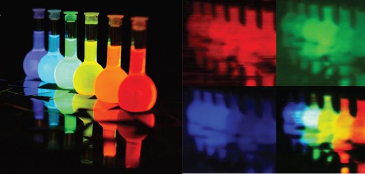
Original image (left) and corresponding portrayal of the red, green and blue regions, and a composite image. Empa
The human eye has three different types of sensory cells for the perception of colour: cells that are respectively sensitive to red, green and blue alternate in the eye and combine their information to create an overall coloured image. Image sensors, for example in mobile phone cameras, work in a similar way: blue, green and red sensors alternate in a mosaic-like pattern. Intelligent software algorithms calculate a high-resolution colour image from the individual colour pixels.
However, the principle also has some inherent limitations: as each individual pixel can only absorb a small part of the light spectrum that hits it, a large part of the light is lost. In addition, the sensors have basically reached the limits of miniaturisation, and unwanted image disturbances can occur; these are known as colour moiré effects and have to be laboriously removed from the finished image.
Transparent only for certain colours
Researchers have therefore been working for a number of years on the idea of stacking the three sensors instead of placing them next to each other. Of course, this requires that the sensors on top let through the light frequencies that they do not absorb to the sensors underneath. At the end of the 1990s, this type of sensor was successfully produced for the first time. It consisted of three stacked silicon layers, each of which absorbed only one colour.
This actually resulted in a commercially available image sensor. However, this was not successful on the market because the absorption spectra of the different layers were not distinct enough, so part of the green and red light was absorbed by the blue-sensitive layer. The colours therefore blurred and the light sensitivity was thus lower than for ordinary light sensors. In addition, the production of the absorbing silicon layers required a complex and expensive manufacturing process.
Empa researchers have now succeeded in developing a sensor prototype that circumvents these problems. It consists of three different types of perovskites – a semiconducting material that has become increasingly important during the last few years, for example in the development of new solar cells, due to its outstanding electrical properties and good optical absorption capacity.
Depending on the composition of these perovskites, they can, for example, absorb part of the light spectrum, but remain transparent for the rest of the spectrum. The researchers in Maksym Kovalenko's group at Empa and ETH Zurich used this principle to create a colour sensor with a size of just one pixel. The researchers were able to reproduce both simple one-dimensional and more realistic two-dimensional images with an extremely high colour fidelity.
Accurate recognition of colours
The advantages of this new approach are clear: the absorption spectra are clearly differentiated and the colour recognition is thus much more precise than with silicon. In addition, the absorption coefficients, especially for the light components with higher wavelengths (green and red), are considerably higher in the perovskites than in silicon.
As a result, the layers can be made significantly smaller, which in turn allows smaller pixel sizes. This is not crucial in the case of ordinary camera sensors; however, for other analysis technologies, such as spectroscopy, this could permit significantly higher spatial resolution. The perovskites can also be produced using a comparatively cheap process.
However, more work is still needed in order to further develop this prototype into a commercially usable image sensor. Key areas include the miniaturisation of pixels and the development of methods for producing an entire matrix of such pixels in one step. According to Kovalenko, this should be possible with existing technologies.
Further reading
Perovskites are such a promising material in research that the prestigious journal Science has published a special edition about them. It includes a review article by the Empa/ETH research group led by Maksym Kovalenko about the current state of research and potential uses of lead halide perovskites nanocrystals.
These have properties that make them a promising candidate for the development of semiconductor nanocrystals for various optoelectronic applications such as television screens, LEDs and solar cells: they are inexpensive to manufacture, have a high tolerance to defects and can be tuned precisely to emit light in a specific colour spectrum.
The paper was published on 10 November.
M Kovalenko, L Protesescu, MI Bodnarchuk
“Properties and potential optoelectronic applications of lead halide perovskites nanocrystals” (Science, 2017)
DOI: 10.1126/science.aam7093
Media Contact
All latest news from the category: Materials Sciences
Materials management deals with the research, development, manufacturing and processing of raw and industrial materials. Key aspects here are biological and medical issues, which play an increasingly important role in this field.
innovations-report offers in-depth articles related to the development and application of materials and the structure and properties of new materials.
Newest articles

Hyperspectral imaging lidar system achieves remote plastic identification
New technology could remotely identify various types of plastics, offering a valuable tool for future monitoring and analysis of oceanic plastic pollution. Researchers have developed a new hyperspectral Raman imaging…

SwRI awarded $26 million to develop NOAA magnetometers
SW-MAG data will help NOAA predict, mitigate the effects of space weather. NASA and the National Oceanic and Atmospheric Administration (NOAA) recently awarded Southwest Research Institute a $26 million contract…

Protein that helps cancer cells dodge CAR T cell therapy
Discovery could lead to new treatments for blood cancer patients currently facing limited options. Scientists at City of Hope®, one of the largest and most advanced cancer research and treatment…


