Tuning flexible circuits with light

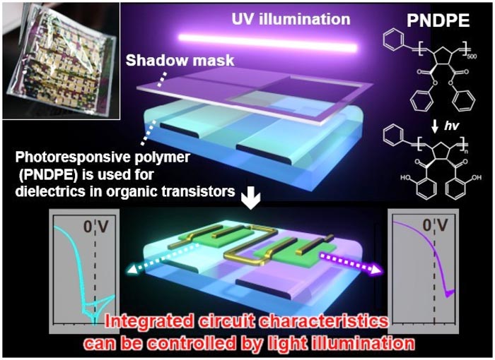
Schematic showing the process that allows for precise control of the organic transistor characteristics using light irradiation. The inset displays a photograph of the final device.
Credit: Takafumi Uemura et al.
Researchers use ultraviolet light to tune circuit performance with a photoreactive polymer based on controlled changes in the chemical structure, which may lead to the development of wearable electronics and medical sensors.
Researchers from SANKEN (The Institute of Scientific and Industrial Research) at Osaka University and JOANNEUM RESEARCH (Weiz, Austria), have shown how exposing an organic polymer to ultraviolet light can precisely modify its electronic properties. This work may aid in the commercialization of flexible electronics that can be used for real-time healthcare monitoring, along with data processing.
While the integrated circuits inside your smart phone are quite impressive, they lack certain important features. Because the electronics are silicon based, they are very rigid, both in the literal sense of being inflexible, as well as having chemical properties that are not easily altered. Newer devices, including OLED displays, are made from carbon-based organic molecules with chemical properties than can be tuned by scientists to produce the most efficient circuits. However, controlling the characteristics of organic transistors usually requires the integration of complex structures made of various materials.
Now, a team of researchers led by Osaka University have used UV light to precisely change the chemical structure of a dielectric polymer called PNDPE. The light breaks specific bonds in the polymer, which can then rearrange into new versions, or create crosslinks between strands. The longer the light is on, the more the polymer get altered. By using a shadow mask, the UV light is applied to just the desired areas, tuning the circuit behavior. This method can pattern transistors of the desired threshold voltage with high spatial resolution using just a single material.
“We have succeeded in controlling the characteristics of organic integrated circuits using persistent light-induced changes in the molecular structure itself,” study corresponding author Takafumi Uemura explains.
In the future, we may see smart versions of almost everything, from medicine bottles to safety vests. “Meeting the computational demands of ‘the Internet of Things’ will very likely require flexible electronic solutions,” senior author Tsuyoshi Sekitani says. In particular, this technology can be applied to manufacturing methods for ultra-lightweight wearable healthcare devices.
The article, “Heterogeneous functional dielectric patterns for charge carrier modulation in ultraflexible organic integrated circuits” was published in Advanced Materials at DOI: https://onlinelibrary.wiley.com/doi/10.1002/adma.202104446
About Osaka University
Osaka University was founded in 1931 as one of the seven imperial universities of Japan and is now one of Japan’s leading comprehensive universities with a broad disciplinary spectrum. This strength is coupled with a singular drive for innovation that extends throughout the scientific process, from fundamental research to the creation of applied technology with positive economic impacts. Its commitment to innovation has been recognized in Japan and around the world, being named Japan’s most innovative university in 2015 (Reuters 2015 Top 100) and one of the most innovative institutions in the world in 2017 (Innovative Universities and the Nature Index Innovation 2017). Now, Osaka University is leveraging its role as a Designated National University Corporation selected by the Ministry of Education, Culture, Sports, Science and Technology to contribute to innovation for human welfare, sustainable development of society, and social transformation.
Website: https://resou.osaka-u.ac.jp/en
About JOANNEUM RESEARCH
JOANNEUM RESEARCH develops solutions and technologies for a broad range of industries and public agencies and is engaged in top applied research at an international level. Optimally embedded in the national and international innovation network our staff develops innovations in the three thematic areas of information and production technologies, human technology and medicine, society and sustainability.
Using modern technologies and processes based on miniaturisation, integration and material optimisation, MATERIALS – The Institute for Surface Technologies and Photonics – offers interdisciplinary solutions for the entire value chain. These include large-area micro- and nanostructures, bio- and chemosensors, light technologies, functionalised surfaces or laser processes.
Website: www.joanneum.at/materials
Journal: Advanced Materials
DOI: 10.1002/adma.202104446
Method of Research: Experimental study
Subject of Research: Not applicable
Article Title: Heterogeneous functional dielectric patterns for charge carrier modulation in ultraflexible organic integrated circuits
Article Publication Date: 21-Sep-2021
Media Contact
Saori Obayashi
Osaka University
gi-strategy@cgin.osaka-u.ac.jp
Office: 81-661-055-886
All latest news from the category: Materials Sciences
Materials management deals with the research, development, manufacturing and processing of raw and industrial materials. Key aspects here are biological and medical issues, which play an increasingly important role in this field.
innovations-report offers in-depth articles related to the development and application of materials and the structure and properties of new materials.
Newest articles

Innovative 3D printed scaffolds offer new hope for bone healing
Researchers at the Institute for Bioengineering of Catalonia have developed novel 3D printed PLA-CaP scaffolds that promote blood vessel formation, ensuring better healing and regeneration of bone tissue. Bone is…

The surprising role of gut infection in Alzheimer’s disease
ASU- and Banner Alzheimer’s Institute-led study implicates link between a common virus and the disease, which travels from the gut to the brain and may be a target for antiviral…

Molecular gardening: New enzymes discovered for protein modification pruning
How deubiquitinases USP53 and USP54 cleave long polyubiquitin chains and how the former is linked to liver disease in children. Deubiquitinases (DUBs) are enzymes used by cells to trim protein…


