Blue phosphorus — mapped and measured for the first time

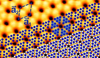
The STM image shows blue phosphorus on a gold substrate. The calculated atomic positions of the slightly elevated P atoms are shown in blue, the lower lying ones in white. Groups of six elevated P atoms appear as triangles. Credit: HZB
In this form, the phosphorus atoms arrange in a honeycomb structure similar to graphene, however, not completely flat but regularly “buckled”.
Model calculations showed that blue phosphorus is not a narrow gap semiconductor like black phosphorus in the bulk but possesses the properties of a semiconductor with a rather large band gap of 2 electron volts. This large gap, which is seven times larger than in bulk black phosphorus, is important for optoelectronic applications.
Blue P examined at BESSY II
In 2016, blue phosphorus was successfully stabilized on a gold substrate by evaporation. Nevertheless, only now we know for certain that the resulting material is indeed blue phosphorus. To this end, a team from HZB around Evangelos Golias has probed the electronic band structure of the material at BESSY II.
They were able to measure by angle-resolved photoelectron spectroscopy the distribution of electrons in its valence band, setting the lower limit for the band gap of blue phosphorus.
Band structure influenced by the substrate
They found that the P atoms do not arrange independently of the gold substrate but try to adjust to the spacings of the Au atoms. This distorts the corrugated honeycomb lattice in a regular manner which in turn affects the behavior of electrons in blue phosphorus.
As a result, the top of the valence band that defines the one end of the semiconducting band gap agrees with the theoretical predictions about its energy position but is somewhat shifted.
Outlook: optoelectronic applications
“So far, researchers have mainly used bulk black phosphorus to exfoliate atomically thin layers”, Prof. Oliver Rader, head of HZB-Department Materials for green spintronics explains. “These also show a large semiconducting band gap but do not possess the honeycomb structure of blue phosphorus and, above all, cannot be grown directly on a substrate.
Our work not only reveals all the material properties of this novel two-dimensional phosphorus allotrope but highlights the impact of the supporting substrate on the behavior of electrons in blue phosphorus, an essential parameter for any optoelectronic application.”
Media Contact
All latest news from the category: Physics and Astronomy
This area deals with the fundamental laws and building blocks of nature and how they interact, the properties and the behavior of matter, and research into space and time and their structures.
innovations-report provides in-depth reports and articles on subjects such as astrophysics, laser technologies, nuclear, quantum, particle and solid-state physics, nanotechnologies, planetary research and findings (Mars, Venus) and developments related to the Hubble Telescope.
Newest articles

Pinpointing hydrogen isotopes in titanium hydride nanofilms
Although it is the smallest and lightest atom, hydrogen can have a big impact by infiltrating other materials and affecting their properties, such as superconductivity and metal-insulator-transitions. Now, researchers from…

A new way of entangling light and sound
For a wide variety of emerging quantum technologies, such as secure quantum communications and quantum computing, quantum entanglement is a prerequisite. Scientists at the Max-Planck-Institute for the Science of Light…

Telescope for NASA’s Roman Mission complete, delivered to Goddard
NASA’s Nancy Grace Roman Space Telescope is one giant step closer to unlocking the mysteries of the universe. The mission has now received its final major delivery: the Optical Telescope…


