Getting electrons to move in a semiconductor

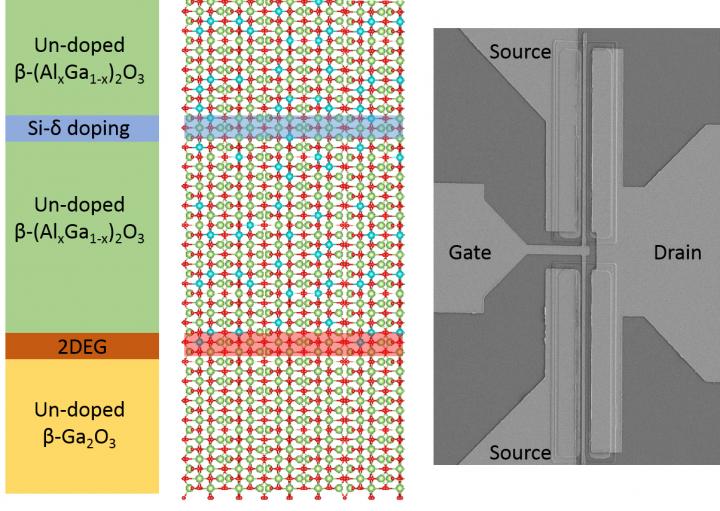
Schematic stack and the scanning electron microscopic image of the β-(AlxGa1-x)2O3/Ga2O3 modulation-doped field effect transistor. Credit: Choong Hee Lee and Yuewei Zhang
The next generation of energy-efficient power electronics, high-frequency communication systems, and solid-state lighting rely on materials known as wide bandgap semiconductors. Circuits based on these materials can operate at much higher power densities and with lower power losses than silicon-based circuits. These materials have enabled a revolution in LED lighting, which led to the 2014 Nobel Prize in physics.
In new experiments reported in Applied Physics Letters, from AIP Publishing, researchers have shown that a wide-bandgap semiconductor called gallium oxide (Ga2O3) can be engineered into nanometer-scale structures that allow electrons to move much faster within the crystal structure.
With electrons that move with such ease, Ga2O3 could be a promising material for applications such as high-frequency communication systems and energy-efficient power electronics.
“Gallium oxide has the potential to enable transistors that would surpass current technology,” said Siddharth Rajan of Ohio State University, who led the research.
Because Ga2O3 has one of the largest bandgaps (the energy needed to excite an electron so that it's conductive) of the wide bandgap materials being developed as alternatives to silicon, it's especially useful for high-power and high-frequency devices. It's also unique among wide bandgap semiconductors in that it can be produced directly from its molten form, which enables large-scale manufacturing of high-quality crystals.
For use in electronic devices, the electrons in the material must be able to move easily under an electric field, a property called high electron mobility. “That's a key parameter for any device,” Rajan said. Normally, to populate a semiconductor with electrons, the material is doped with other elements. The problem, however, is that the dopants also scatter electrons, limiting the electron mobility of the material.
To solve this problem, the researchers used a technique known as modulation doping. The approach was first developed in 1979 by Takashi Mimura to create a gallium arsenide high-electron mobility transistor, which won the Kyoto Prize in 2017. While it is now a commonly used technique to achieve high mobility, its application to Ga2O3 is something new.
In their work, the researchers created a so-called semiconductor heterostructure, creating an atomically perfect interface between Ga2O3 and its alloy with aluminum, aluminum gallium oxide — two semiconductors with the same crystal structure but different energy gaps. A few nanometers away from the interface, embedded inside the aluminum gallium oxide, is a sheet of electron-donating impurities only a few atoms thick.
The donated electrons transfer into the Ga2O3, forming a 2-D electron gas. But because the electrons are now also separated from the dopants (hence the term modulation doping) in the aluminum gallium oxide by a few nanometers, they scatter much less and remain highly mobile.
Using this technique, the researchers reached record mobilities. The researchers were also able to observe Shubnikov-de Haas oscillations, a quantum phenomenon in which increasing the strength of an external magnetic field causes the resistance of the material to oscillate. These oscillations confirm formation of the high mobility 2-D electron gas and allow the researchers to measure critical material properties.
Rajan explained that such modulation-doped structures could lead to a new class of quantum structures and electronics that harnesses the potential of Ga2O3.
###
The article, “Demonstration of high mobility and quantum transport in modulation-doped β-(AlxGa1-x)2O3/Ga2O3 heterostructures,” is authored by Yuewei Zhang, Adam Neal, Zhanbo Xia, Chandan Joishi, Yuanhua Zheng, Sanyam Bajaj, Mark Brenner, Shin Mou, Donald Dorsey, Kelson Chabak, Gregg Jessen, Jinwoo Hwang, Joseph Heremans and Siddarth Rajan. The article will appear in Applied Physics Letters April 24, 2018 (DOI: 10.1063/1.5025704). After that date, it can be accessed at http://aip.
ABOUT THE JOURNAL
Applied Physics Letters features concise, rapid reports on significant new findings in applied physics. The journal covers new experimental and theoretical research on applications of physics phenomena related to all branches of science, engineering, and modern technology. See http://apl.
Media Contact
More Information:
http://dx.doi.org/10.1063/1.5025704All latest news from the category: Physics and Astronomy
This area deals with the fundamental laws and building blocks of nature and how they interact, the properties and the behavior of matter, and research into space and time and their structures.
innovations-report provides in-depth reports and articles on subjects such as astrophysics, laser technologies, nuclear, quantum, particle and solid-state physics, nanotechnologies, planetary research and findings (Mars, Venus) and developments related to the Hubble Telescope.
Newest articles

First-of-its-kind study uses remote sensing to monitor plastic debris in rivers and lakes
Remote sensing creates a cost-effective solution to monitoring plastic pollution. A first-of-its-kind study from researchers at the University of Minnesota Twin Cities shows how remote sensing can help monitor and…

Laser-based artificial neuron mimics nerve cell functions at lightning speed
With a processing speed a billion times faster than nature, chip-based laser neuron could help advance AI tasks such as pattern recognition and sequence prediction. Researchers have developed a laser-based…

Optimising the processing of plastic waste
Just one look in the yellow bin reveals a colourful jumble of different types of plastic. However, the purer and more uniform plastic waste is, the easier it is to…


