MEMS chips get metatlenses

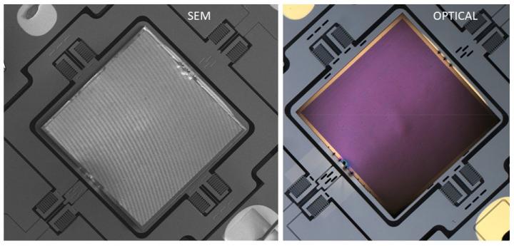
Metasurface-based flat lens integrated onto a MEMS scanner: Scanning electron micrograph (left) and optical microscope image (right) of a lens-on-MEMS device. Integration of MEMS devices with metalenses will help to create a new paradigm to manipulate light by combining the strength of these technologies: high-speed dynamic control with precise spatial manipulation of wave-fronts. Credit: Center for Nanoscale Materials, Argonne National Lab
Lens technologies have advanced across all scales, from digital cameras and high bandwidth in fiber optics to the LIGO lab instruments. Now, a new lens technology that could be produced using standard computer-chip technology is emerging and could replace the bulky layers and complex geometries of traditional curved lenses.
Flat lenses, unlike their traditional counterparts, are relatively lightweight, based on optical nanomaterials known as metasurfaces. When the subwavelength nanostructures of a metasurface form certain repeated patterns, they mimic the complex curvatures that refract light, but with less bulk and an improved ability to focus light with reduced distortion. However, most of these nanostructured devices are static, which limits their functionality.
Federico Capasso, an applied physicist at Harvard University who pioneered metalens technology, and Daniel Lopez, group leader of nanofabrication and devices at Argonne National Laboratory and an early developer of microelectromechanical systems (MEMS), brainstormed about adding motion capabilities like fast scanning and beam steering to metalenses for new applications.
Capasso and Lopez developed a device that integrates mid-infrared spectrum metalenses onto MEMS. The researchers report their findings this week in APL Photonics, from AIP Publishing.
MEMS is a circuit-based technology that incorporates microelectronics, like those found in computer chips, and includes mechanical microstructures like actuators and gears. Ubiquitous in everything from cellphones to airbags, biosensing devices, appliances and optics, MEMS are fabricated using the same techniques used for integrated circuits on typical computer chips.
“Dense integration of thousands of individually controlled lens-on-MEMS devices onto a single silicon chip would allow an unprecedented degree of control and manipulation of the optical field,” Lopez Said.
The researchers formed the metasurface lens using standard photolithography techniques on a silicon-on-insulator wafer with a 2-micron-thick top device layer, a 200-nanometer buried-oxide layer, and a 600-micron-thick handle layer. Then, they placed the flat lens onto a MEMS scanner, essentially a micromirror that deflects light for high-speed optical path length modulation. They aligned the lens with the MEMS' central platform and fixed them together by depositing small platinum patches.
“Our MEMS-integrated metasurface lens prototype can be electrically controlled to vary the angular rotation of a flat lens and can scan the focal spot by several degrees,” Lopez said. “Furthermore, this proof-of-concept integration of metasurface-based flat lenses with MEMS scanners can be extended to the visible and other parts of the electromagnetic spectrum, implying the potential for application across wider fields, such as MEMS-based microscope systems, holographic and projection imaging, LIDAR (light detection and ranging) scanners and laser printing.”
When electrostatically actuated, the MEMS platform controls the angle of the lens along two orthogonal axes, allowing the scanning of the flat lens focal spot by about 9 degrees in each direction. The researchers estimate that the focusing efficiency is about 85 percent.
“Such metalenses can be mass produced with the same computer-chip fabrication technology and in the future, will replace conventional lenses in a wide range of applications,” Capasso said.
###
The article, “Dynamic metasurface lens based on MEMS technology,” is authored by Tapashree Roy, Shuyan Zhang, Il Woong Jung, Mariano Troccoli, Federico Capasso and Daniel Lopez. The article appeared in APL Photonics Feb. 20, 2018 (DOI: 10.1063/1.5018865) and can be accessed at http://aip.
ABOUT THE JOURNAL
APL Photonics is the dedicated home for open access multidisciplinary research from and for the photonics community. The journal publishes fundamental and applied results that significantly advance the knowledge in photonics across physics, chemistry, biology and materials science. See http://aip.
Media Contact
All latest news from the category: Physics and Astronomy
This area deals with the fundamental laws and building blocks of nature and how they interact, the properties and the behavior of matter, and research into space and time and their structures.
innovations-report provides in-depth reports and articles on subjects such as astrophysics, laser technologies, nuclear, quantum, particle and solid-state physics, nanotechnologies, planetary research and findings (Mars, Venus) and developments related to the Hubble Telescope.
Newest articles

NASA: Mystery of life’s handedness deepens
The mystery of why life uses molecules with specific orientations has deepened with a NASA-funded discovery that RNA — a key molecule thought to have potentially held the instructions for…

What are the effects of historic lithium mining on water quality?
Study reveals low levels of common contaminants but high levels of other elements in waters associated with an abandoned lithium mine. Lithium ore and mining waste from a historic lithium…

Quantum-inspired design boosts efficiency of heat-to-electricity conversion
Rice engineers take unconventional route to improving thermophotovoltaic systems. Researchers at Rice University have found a new way to improve a key element of thermophotovoltaic (TPV) systems, which convert heat…


