Quantum Quarry: Scientists Unveil New Technique for Spotting Quantum Dots to Make High Performance Nanophotonic Devices

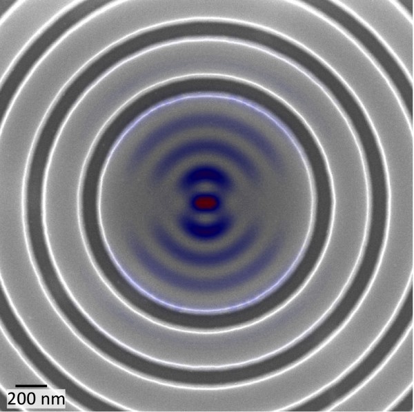
Circular grating geometry for efficiently extracting single photons from a quantum dot.
A quantum dot should produce one and only one photon—the smallest constituent of light—each time it is energized, and this characteristic makes it attractive for use in various quantum technologies, such as secure communications. However, the trick is in finding them.
While they appear randomly, in order for the dots to be useful they need to be located in a precise relation to some other photonic structure, be it a grating, resonator or waveguide, which will enable control of the photons that the quantum dot generates. However, finding the quantum dots—they’re just about 10 nanometers across—is no small feat.
Now, researchers working at the National Institute of Standards and Technology (NIST) in the United States, in collaboration with the universities of Southampton (UK)and Rochester (US), have developed a simple new technique for locating them and used it to create high-performance single photon sources.
This new development, which is published in Nature Communications, may make the manufacture of high-performance photonic devices using quantum dots much more efficient. Such devices are usually made in regular arrays using standard nanofabrication techniques like electron-beam lithography and semiconductor etching.
However because of the random distribution of the dots, only a small percentage of them will line up correctly, at the optimum position within the device. This overall process thus produces very few working devices.
“This is a first step towards providing accurate location information for the manufacture of high performance quantum dot devices,” says NIST physicist Kartik Srinivasan. “So far, the general approach has been statistical – make a lot of devices and end up with a small fraction that work – but our camera-based imaging technique instead seeks to map the location of the quantum dots first, and then uses that knowledge to build optimized light-control devices in the right place.”
Dr Luca Sapienza, from the University’s Quantum Light and Matter group, says: “This new technique is sort of a twist on a red-eye reducing camera flash, where the first flash causes the subject’s pupils to close and the second illuminates the scene.”
In their setup, instead of xenon-powered flash the team used two LEDS. One LED activates the quantum dots when it flashes (you could say this LED gives the quantum dots red eye). At the same time, a second, different color LED flash illuminates metallic orientation marks placed on the surface of the semiconductor wafer the dots are embedded in. Then a sensitive camera snaps a 100-micrometer by 100-micrometer picture.
By cross-referencing the glowing dots with the orientation marks, the researchers can determine the dots’ locations with an uncertainty of less than 30 nanometers. Their coordinates in hand, scientists can then tell the computer-controlled electron beam lithography tool to place any structure the application calls for in its proper relation to the quantum dots, resulting in many more usable devices.
Using this technique, the researchers demonstrated grating-based single photon sources in which they were able to collect 50 per cent of the quantum dot’s emitted photons, the theoretical limit for this type of structure.
They also demonstrated that more than 99 per cent of the light produced from their source came out as single photons. Such high purity is partly due to the fact that the location technique helps the researchers to quickly survey the wafer (10,000 square micrometers at a time) to find regions where the quantum dot density is especially low–only about one per 1,000 square micrometers. This makes it far more likely that each grating device contains one—and only one—quantum dot.
This work was performed in part at NIST’s Center for Nanoscale Science and Technology (CNST), a national user facility available to researchers from industry, academia and government.
Ends
Notes for editors:
1. L. Sapienza, M. Davanço, A. Badolato and K. Srinivasan. Nanoscale optical positioning of single quantum dots for bright and pure single-photon emission. Nature Communications, 6, 7833 doi:10.1038/ncomms8833. Published 27 July 2015.
2. The attached image shows circular grating geometry for efficiently extracting single photons from a quantum dot.
3. Through world-leading research and enterprise activities, the University of Southampton connects with businesses to create real-world solutions to global issues. Through its educational offering, it works with partners around the world to offer relevant, flexible education, which trains students for jobs not even thought of. This connectivity is what sets Southampton apart from the rest; we make connections and change the world. http://www.southampton.ac.uk/
http://www.southampton.ac.uk/weareconnected
#weareconnected
For further information:
Glenn Harris, Media Relations, University of Southampton, Tel 023 8059 3212, email G.Harris@soton.ac.uk, Twitter: @glennh75
www.soton.ac.uk/mediacentre/
Follow us on twitter: http://twitter.com/unisouthampton
Like us on Facebook: www.facebook.com/unisouthampton
Contact Information
Steve Williams
Media Contact
s.williams@soton.ac.uk
Media Contact
All latest news from the category: Physics and Astronomy
This area deals with the fundamental laws and building blocks of nature and how they interact, the properties and the behavior of matter, and research into space and time and their structures.
innovations-report provides in-depth reports and articles on subjects such as astrophysics, laser technologies, nuclear, quantum, particle and solid-state physics, nanotechnologies, planetary research and findings (Mars, Venus) and developments related to the Hubble Telescope.
Newest articles

First-of-its-kind study uses remote sensing to monitor plastic debris in rivers and lakes
Remote sensing creates a cost-effective solution to monitoring plastic pollution. A first-of-its-kind study from researchers at the University of Minnesota Twin Cities shows how remote sensing can help monitor and…

Laser-based artificial neuron mimics nerve cell functions at lightning speed
With a processing speed a billion times faster than nature, chip-based laser neuron could help advance AI tasks such as pattern recognition and sequence prediction. Researchers have developed a laser-based…

Optimising the processing of plastic waste
Just one look in the yellow bin reveals a colourful jumble of different types of plastic. However, the purer and more uniform plastic waste is, the easier it is to…


