Scientists from the UAB and ICMAB achieve unprecedented control of formation of nanostructures

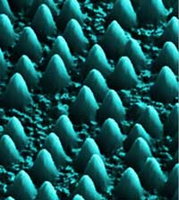
Atomic Force Microscope image of nanoislands
A team of researchers from the Universitat Autònoma de Barcelona, together with researchers from ICMAB (CSIC) and other Russian and Ukrainian scientists, have discovered an unprecedented method for accurately controlling the formation of nanometric structures made of semiconducting material in the form of islets, using promising optoelectronic applications in the most advanced communication technology. The discovery was featured as a cover story by the prestigious Nanotechnology magazine.
One of the areas that is currently being most thoroughly researched with respect to future applications is the manipulation of surfaces on a nanometric scale, up to the point of practically constructing and manipulating structures atom by atom, and whereby the quantum effects could give these materials new properties, with revolutionary applications for nanoelectronics, optoelectronics and computing. One of these structures is the so-called quantum dot, in which electrons lose their capacity for mobility in spatial dimensions and become confined to a zero dimension (a dot). At the moment, the experiments with semiconductor materials most similar to quantum dots are the formation of nanoilles, semiconductor islets of several tens of nanometers of diameter and height. These islets can be produced using lithographic techniques, “printing” them onto the surface of a substrate, but for a decade now, scientists have been working on a new, and more efficient and stable, method for constructing them: the spontaneous formation of nanoilles.
Now, a team of researchers from the Universitat Autònoma de Barcelona, together with researchers from the Institute of the Science of Materials in Barcelona (a CSIC institute on the UAB campus), the Institute of Microstructure Physics in Nizhny Novgorod (Russia) and the Institute of Semiconductor Physics in Kiev (Ukraine), have developed unprecedented accuracy in the control of the growth of nanoilles. These researchers have made a detailed study of the spontaneous formation of SiGe nanoilles (semiconductor material) by depositing thin layers of geranium atoms onto silicon substrates, and have observed, for the first time, how they separately affect the thickness of the layers of geranium and the temperature of formation of nanoilles in their distribution, composition and in two possible forms: pyramid or rounded.
The team of researchers has developed an unprecedented level of control of the distribution, shape and composition of the SiGe nanoilles, such that by varying the thickness of the layers of geranium and the temperature of the silicon substrate they can obtain, at will, large densities of small pyramid islets, large round islets distributed at much lower densities or even a uniform mixture of pyramid and rounded islets. As for the control of the composition of the islets’ SiGe semiconductor material, the researchers have observed that as temperature is increased, so does the silicon content, independently of the form and distribution of the nanoilles.
This research was later considered worthy of being the cover story in the prestigious Nanotechnology magazine, and may have important implications for the fields of nanoelectronics and optoelectronics, as semiconductor lasers (such as those used in ‘laser pointers’) manufactured with this material could emit light in a far wider range of colours than at present. It is expected that this discovery will improve the transmission of information via fibre optics and in electronic circuits, the basis of new communication technologies.
The researchers are now working on the formation of other quantum nanostructures, most particularly semiconductor nanolagoons, which are formed spontaneously on depositing layers of cadmium selenium (CdSe) onto zinc selenium (ZnSe) substrates.
Media Contact
All latest news from the category: Physics and Astronomy
This area deals with the fundamental laws and building blocks of nature and how they interact, the properties and the behavior of matter, and research into space and time and their structures.
innovations-report provides in-depth reports and articles on subjects such as astrophysics, laser technologies, nuclear, quantum, particle and solid-state physics, nanotechnologies, planetary research and findings (Mars, Venus) and developments related to the Hubble Telescope.
Newest articles

First-of-its-kind study uses remote sensing to monitor plastic debris in rivers and lakes
Remote sensing creates a cost-effective solution to monitoring plastic pollution. A first-of-its-kind study from researchers at the University of Minnesota Twin Cities shows how remote sensing can help monitor and…

Laser-based artificial neuron mimics nerve cell functions at lightning speed
With a processing speed a billion times faster than nature, chip-based laser neuron could help advance AI tasks such as pattern recognition and sequence prediction. Researchers have developed a laser-based…

Optimising the processing of plastic waste
Just one look in the yellow bin reveals a colourful jumble of different types of plastic. However, the purer and more uniform plastic waste is, the easier it is to…


