Silicon as a semiconductor: silicon carbide would be much more efficient

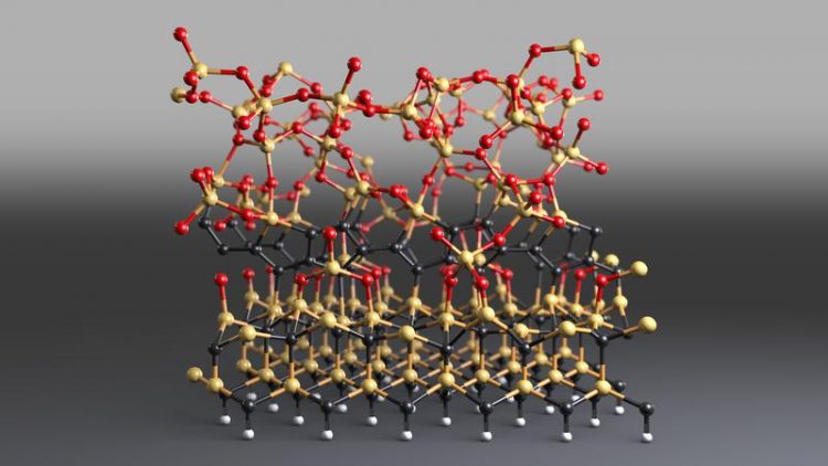
At the interface between silicon dioxide and silicon carbide, irregular clusters of carbon rings occur, which disturb the electronic function. University of Basel, Departement Physik/Swiss Nanoscience Institute
Energy consumption is growing across the globe; electric power is being relied upon more and more, and sustainable energy supplies such as wind and solar power are becoming increasingly important. Electric power, however, is often generated a long distance away from the consumer.
Efficient distribution and transport systems are thus just as crucial as transformer stations and power converters that turn the generated direct current into alternating current.
Huge savings are possible
Modern power electronics must be able to handle large currents and high voltages. Current transistors made of semiconductor materials for field-effect transistors are now mainly based on silicon technology.
Significant physical and chemical advantages, however, arise from the use of SiC over silicon: in addition to a much higher heat resistance, this material provides significantly better energy efficiency, which could lead to massive savings.
It is known that these advantages are significantly compromised by defects at the interface between silicon carbide and the insulating material silicon dioxide. This damage is based on tiny, irregular clusters of carbon rings bound in the crystal lattice, as experimentally demonstrated by researchers led by Professor Thomas Jung at the Swiss Nanoscience Institute and Department of Physics from the University of Basel and the Paul Scherrer Institute. Using atomic force microscope analysis and Raman spectroscopy, they showed that the defects are generated in the vicinity of the interface by the oxidation process.
Experimentally confirmed
The interfering carbon clusters, which are only a few nanometers in size, are formed during the oxidation process of silicon carbide to silicon dioxide under high temperatures. “If we change certain parameters during oxidation, we can influence the occurrence of the defects,” says doctoral student Dipanwita Dutta. For example, a nitrous oxide atmosphere in the heating process leads to significantly fewer carbon clusters.
The experimental results were confirmed by the team led by Professor Stefan Gödecker (Department of Physics and Swiss Nanoscience Institute, University of Basel). Computer simulations confirmed the structural and chemical changes induced by graphitic carbon atoms as observed experimentally. Beyond experiments, atomistic insight has been gained in the generation of the defects and their impact on the electron flow in the semiconductor material.
Better use of electricity
“Our studies provide important insight to drive the onward development of field-effect transistors based on silicon carbide. Therefore we expect to provide a significant contribution to the more effective use of electrical power,” comments Jung. The work was initiated as part of the Nano Argovia program for applied research projects.
Prof. Dr. Thomas Jung, University of Basel, Department of Physics/Swiss Nanoscience Institute; Paul-Scherrer-Institute, Laboratory for Micro and Nanotechnology, phone +41 56 310 45 18; cell: +41 79 222 45 36, email: thomas.jung@unibas.ch
D. Dutta, D. S. De, D. Fan, S. Roy, G. Alfieri, M. Camarda, M. Amsler, J. Lehmann, H. Bartolf, S. Goedecker, T. A. Jung
Evidence for carbon clusters present near thermal gate oxides affecting the electronic band structure in SiC-MOSFET
Applied Physics Letters (2019), doi: 10.1063/1.5112779
Media Contact
More Information:
http://www.unibas.chAll latest news from the category: Physics and Astronomy
This area deals with the fundamental laws and building blocks of nature and how they interact, the properties and the behavior of matter, and research into space and time and their structures.
innovations-report provides in-depth reports and articles on subjects such as astrophysics, laser technologies, nuclear, quantum, particle and solid-state physics, nanotechnologies, planetary research and findings (Mars, Venus) and developments related to the Hubble Telescope.
Newest articles

First-of-its-kind study uses remote sensing to monitor plastic debris in rivers and lakes
Remote sensing creates a cost-effective solution to monitoring plastic pollution. A first-of-its-kind study from researchers at the University of Minnesota Twin Cities shows how remote sensing can help monitor and…

Laser-based artificial neuron mimics nerve cell functions at lightning speed
With a processing speed a billion times faster than nature, chip-based laser neuron could help advance AI tasks such as pattern recognition and sequence prediction. Researchers have developed a laser-based…

Optimising the processing of plastic waste
Just one look in the yellow bin reveals a colourful jumble of different types of plastic. However, the purer and more uniform plastic waste is, the easier it is to…


