A SOI wafer is a suitable substrate for gallium nitride crystals

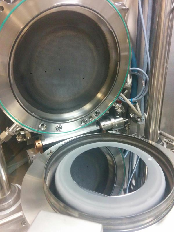
The researchers used Micronova's cleanrooms and, in particular, a reactor designed for gallium nitride manufacturing. The image shows a six-inch substrate in the MOVPE reactor before manufacturing. Credit: Aalto University / Jori Lemettinen
In cooperation with Okmetic Oy and the Polish ITME, researchers at Aalto University have studied the application of SOI (Silicon On Insulator) wafers, which are used as a platform for manufacturing different microelectronics components, as a substrate for producing gallium nitride crystals.
The researchers compared the characteristics of gallium nitride (GaN) layers grown on SOI wafers to those grown on silicon substrates more commonly used for the process. In addition to high-performance silicon wafers, Okmetic also manufactures SOI wafers, in which a layer of silicon dioxide insulator is sandwiched between two silicon layers. The objective of the SOI technology is to improve the capacitive and insulating characteristics of the wafer.
“We used a standardised manufacturing process for comparing the wafer characteristics. GaN growth on SOI wafers produced a higher crystalline quality layer than on silicon wafers. In addition, the insulating layer in the SOI wafer improves breakdown characteristics, enabling the use of clearly higher voltages in power electronics. Similarly, in high frequency applications, the losses and crosstalk can be reduced”, explains Jori Lemettinen, a doctoral candidate from the Department of Electronics and Nanoengineering.
'GaN based components are becoming more common in power electronics and radio applications. The performance of GaN based devices can be improved by using a SOI wafer as the substrate', adds Academy Research Fellow Sami Suihkonen.
SOI wafers reduce the challenges of crystal growth
Growth of GaN on a silicon substrate is challenging. GaN layers and devices can be grown on substrate material using metalorganic vapor phase epitaxy (MOVPE). When using silicon as a substrate the grown compound semiconductor materials have different coefficients of thermal expansion and lattice constants than a silicon wafer. These differences in their characteristics limit the crystalline quality that can be achieved and the maximum possible thickness of the produced layer.
'The research showed that the layered structure of an SOI wafer can act as a compliant substrate during gallium nitride layer growth and thus reduce defects and strain in the grown layers”, Lemettinen notes. GaN based components are commonly used in blue and white LEDs. In power electronics applications, GaN diodes and transistors, in particular, have received interest, for example in frequency converters or electric cars. It is believed that in radio applications, 5G network base stations will use GaN based power amplifiers in the future. In electronics applications, a GaN transistor offers low resistance and enables high frequencies and power densities.
###
The article has been accepted for publication in the journal Semiconductor Science and Technology. Link to the article https:/
Further information:
Jori Lemettinen
Aalto University
jori.lemettinen@aalto.fi
tel. +358 40 5723 087
Academy Research Fellow Sami Suihkonen
Aalto University
sami.suihkonen@aalto.fi
tel. +358 50 3618 657
Media Contact
All latest news from the category: Power and Electrical Engineering
This topic covers issues related to energy generation, conversion, transportation and consumption and how the industry is addressing the challenge of energy efficiency in general.
innovations-report provides in-depth and informative reports and articles on subjects ranging from wind energy, fuel cell technology, solar energy, geothermal energy, petroleum, gas, nuclear engineering, alternative energy and energy efficiency to fusion, hydrogen and superconductor technologies.
Newest articles

First-of-its-kind study uses remote sensing to monitor plastic debris in rivers and lakes
Remote sensing creates a cost-effective solution to monitoring plastic pollution. A first-of-its-kind study from researchers at the University of Minnesota Twin Cities shows how remote sensing can help monitor and…

Laser-based artificial neuron mimics nerve cell functions at lightning speed
With a processing speed a billion times faster than nature, chip-based laser neuron could help advance AI tasks such as pattern recognition and sequence prediction. Researchers have developed a laser-based…

Optimising the processing of plastic waste
Just one look in the yellow bin reveals a colourful jumble of different types of plastic. However, the purer and more uniform plastic waste is, the easier it is to…


