Atomic precision: technologies for the next-but-one generation of microchips

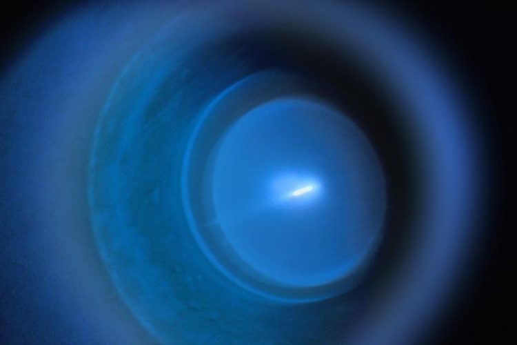
Image 1: The photo shows a discharge generated plasma. © Fraunhofer ILT, Aachen, Germany.
In 1965 Gordon Moore formulated the law that came to be named after him, which states that the complexity of integrated circuits doubles every one to two years. At that time he was regarded as a visionary and pioneering thinker. Today, over 50 years later, we see that the integration density of electronic circuits is still continuing to grow.
Now we can store whole libraries on a chip in our smartphones. That was primarily made possible by revolutionary advances in optical technologies and materials science. And although it’s becoming apparent that there are physical limits, developments are not over yet: scientists at Fraunhofer Institutes in Jena and Aachen are working on the next generation of technology for producing even smaller structures.
New target materials for the 6.7 nm radiation source
A key constraint for the lithographic production of ever smaller structures is the wavelength of the light used. In the 1970s the UV light from a mercury vapor lamp was sufficient; the 1990s saw the emergence of excimer lasers with wavelengths of 193 nm. Today, the semiconductor industry combines these radiation sources with refined methods of optical lithography to manufacture structures as small as 14 nm across.
EUV lithography is a completely new technology that has been developed over the last ten years. It works by using extreme ultraviolet (EUV) radiation at a wavelength of 13.5 nm, which is generated by evaporating a droplet of tin with a high-power laser. The aim is to harness the emitted EUV radiation to produce structures with a size of 10 nm or less.
Having played a leading part in developing EUV technology, scientists at Fraunhofer ILT are now focused on the next step: technology that uses radiation with a wavelength of around 6.7 nm. Instead of tin, they are working with targets made of gadolinium or terbium alloys, as these facilitate correspondingly shorter wavelengths.
Teams from the two Fraunhofer Institutes worked together to develop a new optical system with which to characterize the radiation source. This system enables them to measure factors such as light output to a high degree of spatial and spectral resolution.
The output power of the radiation source is now enough to carry out trials on new mirror coatings or light-sensitive varnishes (resists). Development work on the radiation source is ongoing to achieve the necessary power scaling.
Coating mirrors with atomic precision
Unlike traditional optical lithography, EUV lithography functions use only reflective optics; this means the mirrors have to meet extremely exacting requirements. Nowadays the thickness of mirror coatings must be correct to around 10 picometers. That is less than the diameter of an atom.
It is laborious and expensive to generate EUV radiation, and consequently every percentage point of reflectivity matters. In the case of mirrors for 13 nm radiation, it has been possible to achieve a reflectivity of around 65% using alternating films of silicon and molybdenum. When it comes to mirrors for 6.7 nm radiation, experts from Fraunhofer IOF in Jena have developed special systems using lanthanum and boron compounds. Here, too, they are battling to reach the theoretical limit of around 70%.
Applications in many areas
Today there are already more mobile telephones than human beings on Earth – a fact that was partly made possible by enormous advances in microlithography. This field will continue to be of the utmost importance over the coming years, including for new subject areas such as industry 4.0 or the Internet of Things.
That is why experts from the Fraunhofer Institutes for Applied Optics and Precision Engineering IOF and for Laser Technology ILT have been working since the start of 2014 on developing the basic principles for lithography at even shorter wavelengths. They are collaborating with industrial partners Carl Zeiss SMT and ASML in the “Beyond EUV” project, which runs to the end of 2016, to develop key components for 6.7 nm wavelength technology.
These new lithographic techniques will make it possible to produce structures with a thickness of just a few atoms. There are already lots of ideas for how to use integrated circuits formed from such structures: alongside even higher storage capacity for cloud applications and big data processes, they could also be used for mind-controlled prosthetic limbs or more personalized medicine.
Contact
Dr. rer. nat Klaus Bergmann
Group Manager EUV Technology
Telephone +49 241 8906-302
klaus.bergmann@ilt.fraunhofer.de
Fraunhofer Institute for Laser Technology ILT, Aachen, Germany
Prof. Dr. Norbert Kaiser
Head of Optical Coatings
Telephone +49 3641 807-321
norbert.kaiser@iof.fraunhofer.de
Fraunhofer Institute for Applied Optics and Precision Engineering IOF, Jena, Germany |
http://www.ilt.fraunhofer.de/en.html
http://www.iof.fraunhofer.de/en.html
Media Contact
All latest news from the category: Power and Electrical Engineering
This topic covers issues related to energy generation, conversion, transportation and consumption and how the industry is addressing the challenge of energy efficiency in general.
innovations-report provides in-depth and informative reports and articles on subjects ranging from wind energy, fuel cell technology, solar energy, geothermal energy, petroleum, gas, nuclear engineering, alternative energy and energy efficiency to fusion, hydrogen and superconductor technologies.
Newest articles

First-of-its-kind study uses remote sensing to monitor plastic debris in rivers and lakes
Remote sensing creates a cost-effective solution to monitoring plastic pollution. A first-of-its-kind study from researchers at the University of Minnesota Twin Cities shows how remote sensing can help monitor and…

Laser-based artificial neuron mimics nerve cell functions at lightning speed
With a processing speed a billion times faster than nature, chip-based laser neuron could help advance AI tasks such as pattern recognition and sequence prediction. Researchers have developed a laser-based…

Optimising the processing of plastic waste
Just one look in the yellow bin reveals a colourful jumble of different types of plastic. However, the purer and more uniform plastic waste is, the easier it is to…


