Silicon has been the workhorse of electronics for decades because it is a common element, is easy to process, and has useful electronic properties. A limitation of silicon is that high temperatures damage it, which limits the operating speed of silicon-based electronics. Single-crystal diamond is a possible alternative to silicon. Researchers recently fabricated a single-crystal diamond wafer, but common methods of polishing the surface–a requirement for use in electronics–are a combination of slow and damaging.
In a study recently published in Scientific Reports, researchers from Osaka University and collaborating partners polished a single-crystal diamond wafer to be nearly atomically smooth. This procedure will be useful for helping diamond replace at least some of the silicon components of electronic devices.
Diamond is the hardest known substance and essentially does not react with chemicals. Polishing it with a similarly hard tool damages the surface and conventional polishing chemistry is slow. In this study, the researchers in essence first modified the quartz glass surface and then polished diamond with modified quartz glass tools.
“Plasma-assisted polishing is an ideal technique for single-crystal diamond,” explains lead author Nian Liu. “The plasma activates the carbon atoms on the diamond surface without destroying the crystal structure, which lets a quartz glass plate gently smooth away surface irregularities.”
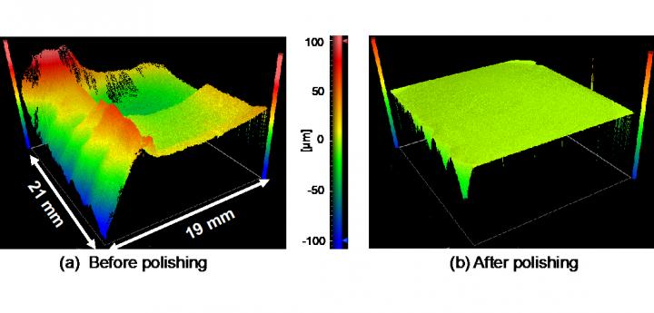
The single-crystal diamond, before polishing, had many step-like features and was wavy overall, with an average root mean square roughness of 0.66 micrometers. After polishing, the topographical defects were gone, and the surface roughness was far less: 0.4 nanometers.
“Polishing decreased the surface roughness to near-atomic smoothness,” says senior author Kazuya Yamamura. “There were no scratches on the surface, as seen in scaife mechanical smoothing approaches.”
Furthermore, the researchers confirmed that the polished surface was unaltered chemically. For example, they detected no graphite–therefore, no damaged carbon. The only detected impurity was a very small amount of nitrogen from the original wafer preparation.
“Using Raman spectroscopy, the full width at half maximum of the diamond lines in the wafer were the same, and the peak positions were almost identical,” says Liu. “Other polishing techniques show clear deviations from pure diamond.”
With this research development, high-performance power devices and heat sinks based on single-crystal diamond are now attainable. Such technologies will dramatically lower the power use and carbon input, and improve the performance, of future electronic devices.
###
The article, “Damage-free highly efficient plasma-assisted polishing of a 20-mm square large mosaic single-crystal diamond substrate,” was published in Scientific Reports at DOI: https:/
About Osaka University
Osaka University was founded in 1931 as one of the seven imperial universities of Japan and is now one of Japan’s leading comprehensive universities with a broad disciplinary spectrum. This strength is coupled with a singular drive for innovation that extends throughout the scientific process, from fundamental research to the creation of applied technology with positive economic impacts. Its commitment to innovation has been recognized in Japan and around the world, being named Japan’s most innovative university in 2015 (Reuters 2015 Top 100) and one of the most innovative institutions in the world in 2017 (Innovative Universities and the Nature Index Innovation 2017). Now, Osaka University is leveraging its role as a Designated National University Corporation selected by the Ministry of Education, Culture, Sports, Science and Technology to contribute to innovation for human welfare, sustainable development of society, and social transformation.
Website: https:/


