Graphene “nano-origami” creates tiniest microchips yet

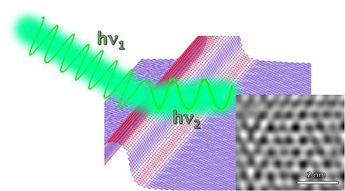
Image reveals the kink in the form of wrinkles that causes change in Raman signals of altered electronic property.
Credit: University of Sussex
Nanomaterial developments could lead to computers and phones running thousands of times faster.
The tiniest microchips yet can be made from graphene and other 2D-materials, using a form of ‘nano-origami’, physicists at the University of Sussex have found.
This is the first time any researchers have done this, and it is covered in a paper published in the ACS Nano journal.
By creating kinks in the structure of graphene, researchers at the University of Sussex have made the nanomaterial behave like a transistor, and have shown that when a strip of graphene is crinkled in this way, it can behave like a microchip, which is around 100 times smaller than conventional microchips.
Prof Alan Dalton in the School of Mathematical and Physics Sciences at the University of Sussex, said:
“We’re mechanically creating kinks in a layer of graphene. It’s a bit like nano-origami.
“Using these nanomaterials will make our computer chips smaller and faster. It is absolutely critical that this happens as computer manufacturers are now at the limit of what they can do with traditional semiconducting technology. Ultimately, this will make our computers and phones thousands of times faster in the future.
“This kind of technology – “straintronics” using nanomaterials as opposed to electronics – allows space for more chips inside any device. Everything we want to do with computers – to speed them up – can be done by crinkling graphene like this.”
Dr Manoj Tripathi, Research Fellow in Nano-structured Materials at the University of Sussex and lead author on the paper, said:
“Instead of having to add foreign materials into a device, we’ve shown we can create structures from graphene and other 2D materials simply by adding deliberate kinks into the structure. By making this sort of corrugation we can create a smart electronic component, like a transistor, or a logic gate.”
The development is a greener, more sustainable technology. Because no additional materials need to be added, and because this process works at room temperature rather than high temperature, it uses less energy to create.
All latest news from the category: Power and Electrical Engineering
This topic covers issues related to energy generation, conversion, transportation and consumption and how the industry is addressing the challenge of energy efficiency in general.
innovations-report provides in-depth and informative reports and articles on subjects ranging from wind energy, fuel cell technology, solar energy, geothermal energy, petroleum, gas, nuclear engineering, alternative energy and energy efficiency to fusion, hydrogen and superconductor technologies.
Newest articles

Innovative 3D printed scaffolds offer new hope for bone healing
Researchers at the Institute for Bioengineering of Catalonia have developed novel 3D printed PLA-CaP scaffolds that promote blood vessel formation, ensuring better healing and regeneration of bone tissue. Bone is…

The surprising role of gut infection in Alzheimer’s disease
ASU- and Banner Alzheimer’s Institute-led study implicates link between a common virus and the disease, which travels from the gut to the brain and may be a target for antiviral…

Molecular gardening: New enzymes discovered for protein modification pruning
How deubiquitinases USP53 and USP54 cleave long polyubiquitin chains and how the former is linked to liver disease in children. Deubiquitinases (DUBs) are enzymes used by cells to trim protein…


