Modeling organic-field effect transistors with a molecular resolution

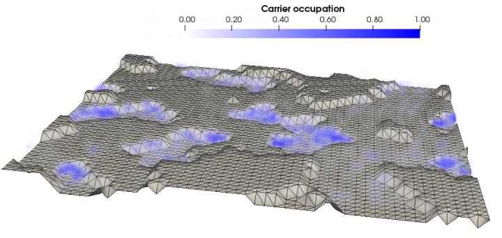
In an OFET, the charge carriers move through the organic semiconductor within a "channel" located at the interface with a dielectric material. Here, the dielectric is represented by the gray grid. The figure illustrates the calculated impact of the roughness of the dielectric surface (showing a 50 nm × 50 nm area) on the averaged carrier occupation The carrier occupation probabilities are represented in blue and indicate that the carriers essentially move within the "valleys" of the dielectric surface (adapted from Adv. Funct. Mater., 2018, 28, 1803096).
Credit: ©Science China Press
Field-effect transistors are key components of sensors, electrical circuits, or data storage devices. The transistors used to date have been mainly based on inorganic semiconductors such as silicon. More recently, organic materials have emerged, with semiconducting properties that have allowed the fabrication of organic field-effect transistors (OFETs).
The use of organic components as the device active layer brings promising features such as easy processing and low cost. In addition to their device functionalities, OFETs have also developed into an important platform in the basic characterization of organic semiconductors, as they are now established as a useful tool to measure charge-carrier mobilities.
Thus, providing a comprehensive description of OFET device performance becomes a key step in furthering the development of these devices and designing more efficient organic semiconductors. At the core of these investigations lie the device models, which provide the relationships between the measured current densities and the semiconducting properties of the organic materials. Needless to say, it is imperative that these OFET device models be accurate and reliable.
In an overview published in the Beijing-based National Science Review, scientists at the University of Arizona in the United States discuss recent advances in OFET device models that incorporate molecular-level parameters. In particular, they highlight the development of kinetic Monte Carlo-based device simulation methods and their successful application to the modeling of micrometer-sized OFETs. They also outline the paths require for further improvements of these molecular-level models for OFETs.
“In spite of the major differences in the charge-transport mechanisms of organic and inorganic semiconductors, it turns out that until recently the prevalent OFET device models were directly borrowed from those originally developed for FETs based on inorganic materials”, these scientists state in their review article entitled “Developing Molecular-Level Models for Organic Field-Effect Transistors.”
They emphasize that: “Optimally, OFET device models should include factors such as the presence of discrete molecular levels, disorder, anisotropy, traps, grain boundaries, complex film morphology, and contact resistance. These factors are difficult to include as long as the organic semiconductor film is treated as a continuum medium. In other words, nano-scale, molecular-level details need to be incorporated into OFET device models.”
In recent years, kinetic Monte Carlo-based methods have seen very substantial developments, which now allows an efficient modeling of OFETs with a molecular resolution. These new models have opened the way to a deeper understanding of the OFET device physics and provided the ability to connect directly the microscopic processes to macroscopic device performance.
They have been successfully applied to describe fundamental aspects of OFETs such as the actual thickness of the effective channel and the impact of the dielectric surface morphology, as well as the issue of nonlinear current characteristics encountered more recently.
The University of Arizona scientists forecast that: “Through such continuous developments, molecular-level OFET device models will become an increasingly useful platform in the investigation of OFET devices and serve as a complementary tool for routine data analysis”.
###
This work has been supported by the University of Arizona and the Georgia Institute of Technology.
See the article:
Haoyuan Li and Jean-Luc Brédas
Developing Molecular-Level Models for Organic Field-Effect Transistors
Natl Sci Rev, DOI: 10.1093/nsr/nwaa167
https:/
The National Science Review is the first comprehensive scholarly journal released in English in China that is aimed at linking the country’s rapidly advancing community of scientists with the global frontiers of science and technology. The journal also aims to shine a worldwide spotlight on scientific research advances across China.
All latest news from the category: Power and Electrical Engineering
This topic covers issues related to energy generation, conversion, transportation and consumption and how the industry is addressing the challenge of energy efficiency in general.
innovations-report provides in-depth and informative reports and articles on subjects ranging from wind energy, fuel cell technology, solar energy, geothermal energy, petroleum, gas, nuclear engineering, alternative energy and energy efficiency to fusion, hydrogen and superconductor technologies.
Newest articles

Scientists transform blood into regenerative materials
… paving the way for personalized, blood-based, 3D-printed implants. Scientists have created a new ‘biocooperative’ material based on blood, which has shown to successfully repair bones, paving the way for…

A new experimental infection model in flies
…offers a fast and cost-effective way to test drugs. Researchers at the Germans Trias i Pujol Research Institute and Hospital have reinforced their leading role in infectious disease research by…

Material developed with novel stretching properties
KIT researchers produce metamaterial with different extension and compression properties than conventional materials. With this material, the working group headed by Professor Martin Wegener at KIT’s Institute of Applied Physics…


