A New Advance in Gallium Nitride Nanowires

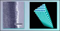
When grown on a substrate of lithium aluminum oxide, gallium nitride nanowires are triangular in cross section.
A significant breakthrough in the development of the highly prized semiconductor gallium nitride as a building block for nanotechnology has been achieved by a team of scientists with the U.S. Department of Energy’s Lawrence Berkeley National Laboratory (Berkeley Lab) and the University of California at Berkeley.
For the first time ever, the researchers have been able control the direction in which a gallium nitride nanowire grows. Growth direction is critical to determining the wire’s electrical and thermal conductivity and other important properties.
“Our results will come as a surprise to those who have said that growth direction can’t be controlled, that you get what you get when you grow semiconductor nanowires,” says Peidong Yang, a chemist with Berkeley Lab’s Materials Sciences Division and a professor with UC Berkeley’s Chemistry Department, who led the research.
A report discussing these research results first appeared in the online edition of the journal Nature Materials on July 25. In addition to Yang, co-authors of the report, “Crystallographic alignment of high-density gallium nitride nanowire arrays,” were Yanfeng Zhang, Donald Sirbuly, and Jonathan Denlinger of Berkeley Lab, and Tevye Kuykendall, Peter Pauzauskie, and Joshua Goldberger of UC Berkeley.
Nanotechnologists are eager to tap into the enormous potential of gallium nitride for use in high-power, high-performance optoelectronic devices. Already, single-crystalline gallium nitride nanowires and nanotubes have shown promise in blue light emitting diodes, short-wavelength ultraviolet nanolasers, and nanofluidic biochemical sensors.
“Control over nanowire growth direction is extremely desirable, in that anisotropic parameters such as thermal and electrical conductivity, index of refraction, piezoelectric polarization, and band gap may be used to tune the physical properties of nanowires made from a given material,” Yang says.
Yang and his research group have been pioneers in the fabrication of semiconductor nanowires, especially gallium nitride, zinc oxide, and silicon/germanium. The wires they’ve produced measure only a few nanometers in diameter but stretch out to several microns in length. For this experimental work, they grew single-crystal gallium nitride nanowires using a metal–organic chemical vapor deposition (MOCVD) technique that was similar to an earlier technique they used to produce nanowire lasers.
In their earlier work, Yang and his group demonstrated the ability to control the size, aspect ratio, position, and composition of their nanowires. Now they’ve added the ability to control crystallographic growth direction. The key to this new capability is the selection of a choice substrate.
Explains Yang, “In nanowires made from the exact same gallium nitride material but grown on different substrates, the light-emission of these wires was blue-shifted by 100 meV (milli-electron volts). We believe the emission difference is a clear manifestation of the different crystal growth directions.”
For this study, Yang and his group used substrates of lithium aluminum oxide and magnesium oxide. The crystals of both materials are geometrically compatible with gallium nitride crystals, but the lithium aluminum oxide features a two-fold symmetry that matches the symmetry along one plane of the gallium nitride crystals, whereas the magnesium oxide has a three-fold symmetry that matches gallium nitride symmetry along a different plane.
As a result, when a vapor of gallium nitride condenses on either of these substrates, the resulting nanowires grow perpendicular to the substrate but aligned in a direction unique to each substrate. Because of the different growth directions, cross sections of the gallium nitride nanowires grown on lithium aluminum oxide form an isosceles triangle, while the cross sections of those grown on magnesium oxide are hexagonal.
“Our goal is to put together a generic scheme for controlling the directional growth of all semiconductor nanowires,” says Yang. “When we can do this, we will be able to answer some important fundamental questions, such as how would the carrier mobility, light emission, and thermoconductivity differ along different crystallographic directions for nanowires with the same compositions and crystal structures. The use of MOCVD for gallium nitride nanowire growth will also allow us to integrate nanowires and thin films of various compositions so we can start making real devices.”
Yang believes that he and his group are within a few months of being able to produce a light-emission diode, a transistor, or a hybrid, nanowire-thin film laser.
This research effort was funded by the U.S. Department of Energy’s Office of Science, the Camille and Henry Dreyfus Foundation, the Beckman Foundation, and the National Science Foundation.
Media Contact
More Information:
http://www.lbl.govAll latest news from the category: Power and Electrical Engineering
This topic covers issues related to energy generation, conversion, transportation and consumption and how the industry is addressing the challenge of energy efficiency in general.
innovations-report provides in-depth and informative reports and articles on subjects ranging from wind energy, fuel cell technology, solar energy, geothermal energy, petroleum, gas, nuclear engineering, alternative energy and energy efficiency to fusion, hydrogen and superconductor technologies.
Newest articles

Innovative 3D printed scaffolds offer new hope for bone healing
Researchers at the Institute for Bioengineering of Catalonia have developed novel 3D printed PLA-CaP scaffolds that promote blood vessel formation, ensuring better healing and regeneration of bone tissue. Bone is…

The surprising role of gut infection in Alzheimer’s disease
ASU- and Banner Alzheimer’s Institute-led study implicates link between a common virus and the disease, which travels from the gut to the brain and may be a target for antiviral…

Molecular gardening: New enzymes discovered for protein modification pruning
How deubiquitinases USP53 and USP54 cleave long polyubiquitin chains and how the former is linked to liver disease in children. Deubiquitinases (DUBs) are enzymes used by cells to trim protein…


