Saving energy by taking a close look inside transistors

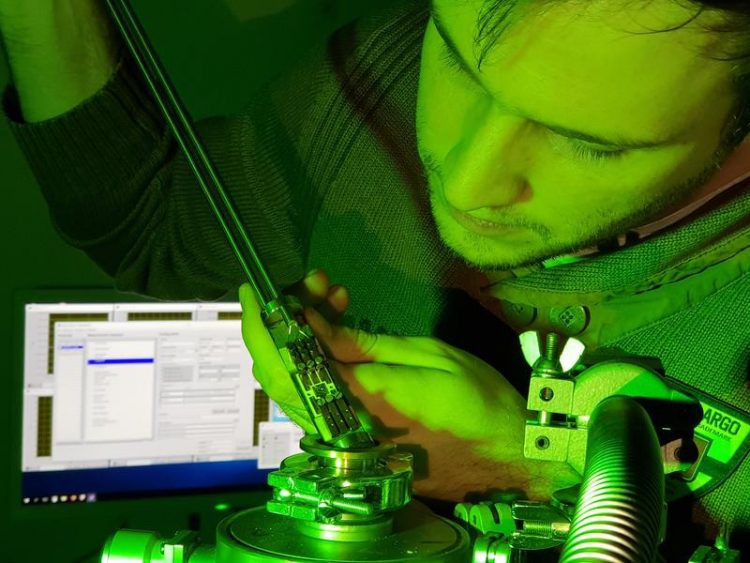
Physicist Martin Hauck fits a silicon carbide transistor into the measuring apparatus: researchers at FAU have discovered a method for finding defects at the interfaces of switches FAU/Michael Krieger, Martin Hauck
Transistors are needed wherever current flows, and they are an indispensable component of virtually all electronic switches. In the field of power electronics, transistors are used to switch large currents.
However, one side-effect is that the components heat up and energy is lost as a result. One way of combating this and potentially making considerable savings is to use energy-efficient transistors. Researchers at Friedrich-Alexander-Universität Erlangen-Nürnberg (FAU) have developed a simple yet accurate method for finding defects in the latest generation of silicon carbide transistors.
This will speed up the process of developing more energy-efficient transistors in future. They have now published their findings in the renowned journal Communications Physics.*
Boosting the efficiency of power electronic devices is one way to save energy in our highly technological world. It is these components which ensure that power from photovoltaic or wind power stations are fed into the grid, the traction units of trains are supplied with current from the overhead line, and energy is transferred from batteries to the engine in electric and hybrid vehicles.
At the same time, however, these components should ideally use as little electricity as possible. If not, heat is generated unnecessarily, additional complex cooling systems are needed and energy is wasted as a result.
This is where components made of silicon, the standard semiconductor material, reach their limits on the basis of their intrinsic material properties. There is, however, a much more suitable alternative: silicon carbide, or SiC for short, a compound made of silicon and carbon.
Its properties speak for themselves: it withstands high voltages, works even at high temperatures, is chemically robust and is able to work at high switching frequencies, which enables even better energy efficiency. SiC components have been used very successfully for several years now.
Investigating charge trapping
Power electronic switches made of silicon carbide, known as field-effect transistors or MOSFETs for short, work on the basis of the interface between the SiC and a very thin layer of silicon oxide which is deposited or grown on it.
It is this interface, however, which poses a significant challenge for researchers: during fabrication, undesired defects are created at the interface which trap charge carriers and reduce the electrical current in the device. Research into these defects is therefore of paramount importance if we are to make full use of the potential offered by the material.
Pattern discovered
Conventional measurement techniques, which have usually been developed with silicon MOSFET devices in mind, simply ignore the existence of such defects. Whilst there are other measurement techniques available, they are more complex and time-consuming, and are either unsuitable for use on a large scale or are simply not suitable for being used on finished components at all. This is the reason why researchers at the Chair of Applied Physics at FAU decided to focus on finding new, improved methods for investigating interface defects – and they were successful.
They noticed that the interface defects always follow the same pattern. ‘We translated this pattern into a mathematical formula,’ explains doctoral candidate Martin Hauck. ‘Using the formula gives us a clever way of taking interface defects into account in our calculations. This doesn’t only give us very precise values for typical device parameters like electron mobility or threshold voltage, it also lets us determine the distribution and density of interface defects almost on the side.
In experiments conducted using transistors specially designed for the purpose by the researchers’ industrial partners Infineon Technologies Austria AG and its subsidiary Kompetenzzentrum für Automobil- & Industrie-Elektronik GmbH, the extremely simple method also proved to be highly accurate.
Taking a close look at the inner core of the field-effect transistors allows now for improved and shorter innovation cycles. Using this method, processes aimed at reducing defects can be evaluated accurately, quickly and simply, and work at developing new, more energy-saving power electronics can be accelerated accordingly.
*doi: https://doi.org/10.1038/s42005-018-0102-8
Further information:
Dr. Michael Krieger
Phone: +49 9131 85-28427
michael.krieger@fau.de
Dr. Michael Krieger
Phone: +49 9131 85-28427
michael.krieger@fau.de
Media Contact
More Information:
http://www.fau.de/All latest news from the category: Power and Electrical Engineering
This topic covers issues related to energy generation, conversion, transportation and consumption and how the industry is addressing the challenge of energy efficiency in general.
innovations-report provides in-depth and informative reports and articles on subjects ranging from wind energy, fuel cell technology, solar energy, geothermal energy, petroleum, gas, nuclear engineering, alternative energy and energy efficiency to fusion, hydrogen and superconductor technologies.
Newest articles

NASA: Mystery of life’s handedness deepens
The mystery of why life uses molecules with specific orientations has deepened with a NASA-funded discovery that RNA — a key molecule thought to have potentially held the instructions for…

What are the effects of historic lithium mining on water quality?
Study reveals low levels of common contaminants but high levels of other elements in waters associated with an abandoned lithium mine. Lithium ore and mining waste from a historic lithium…

Quantum-inspired design boosts efficiency of heat-to-electricity conversion
Rice engineers take unconventional route to improving thermophotovoltaic systems. Researchers at Rice University have found a new way to improve a key element of thermophotovoltaic (TPV) systems, which convert heat…


