Customized layers

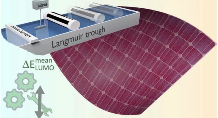
Based on the new „Rolling Transfered Langmuir Layer“ technology, which can be used to produce thin films with specific properties, improved flexible solar cells can be produced, for example.
(c) Leibniz-IPHT
Jena researchers develop new method for manufacturing tailor-made semiconductor thin films.
Organic semiconductor materials are promising key technologies for the development of state-of-the-art optoelectronic components and are used in photovoltaics as well as in sensor technology and microelectronics. In order to produce thin organic semiconductor films automatically and with well-defined properties, researchers – led by Leibniz IPHT in Jena, Germany – have developed a new technological approach for depositing thin films with high molecular precision. The method for manufacturing thin films with tailor-made electronic properties is presented in the journal Advanced Materials.
Organic semiconductors, which usually consist of carbon-based molecular materials or polymers, are part of a variety of today’s applications: For example, ultra-thin, mechanically flexible and lightweight semiconductor thin films are used in modern transistors, sensitive sensors, or organic solar cells. Their energy conversion potential and thus their functionality is determined by the electronic energy levels of the organic thin films, which depend on the molecules as well as their arrangement and the interactions between neighboring molecules within the thin films.
A German-American team of scientists – led by Leibniz Institute of Photonic Technology (Leibniz IPHT) – has succeeded in developing a novel manufacturing process that allows to precisely fabricate thin semiconductor films with customized structural and electronic properties in an automated manner. The method presented in the journal Advanced Materials should make it possible to specifically produce thin films with controllable interactions between neighboring molecules and specific energy levels.
Rolling deposition of semiconductor thin films
The presented “Rolling Transfered Langmuir Layer” technique, a further development of the established Langmuir Blodgett technique for the deposition of thin films, is suitable for the production of monolayers of organic semiconductor molecules at air-water interfaces. For this purpose, a layer of molecules formed on a water surface is transferred to a solid substrate. The molecular monolayer is deposited on the substrate using a specific rolling transfer system developed by the researchers, which contains the substrate to be coated and which is moved over the molecular film on the water surface. The molecular layer formed at the air-water interface adheres to the substrate during the rolling motion.
“The developed process also allows crystalline films to be deposited, the production of which using established methods previously involved considerable effort and often led to surface defects, such as fractures in the organic thin films. With the process presented, we can reduce these surface defects to a minimum and produce both monolayers and multiple thin-film layers with individual properties directly, uniformly and with high quality in a scalable manner,” explains PD Dr. habil. Martin Presselt, head of the Organic Thin Films and Interfaces Group at Leibniz IPHT, who developed the new method together with his team.
Tailor-made thin films
Two parameters play a decisive role in the production of semiconducting thin films with tailor-made structural and energetic properties: “On the one hand, the ‘Rolling Transfered Langmuir Layer’ technique enables to systematically vary the packing density of the molecules within a layer, which can range from very densely packed to less densely packed, via the surface pressure during deposition. On the other hand, the number of stacked molecular layers and thus the layer thickness of the thin films can be precisely adjusted. In this way, semiconductor thin films with targeted interactions between neighboring molecules and specific energy levels can be reproducibly produced,” says Dr. Sarah Jasmin Finkelmeyer, scientist in the Organic Thin Films and Interfaces Group, who played a major role in developing the new method.
The technological approach developed by the researchers lays the foundation for the fabrication of thin-film-based novel (opto-) electronic components with optimized properties. For example, organic photovoltaic modules that efficiently generate electrical energy from sunlight as well as thin films that convert sunlight into chemical energy can be further developed.
About Leibniz Institute of Photonic Technology
Light is at the center of research at Leibniz IPHT. Scientists are researching innovative photonic processes and tools for use in clinical diagnostics, such as infection and cancer diagnostics, pharmacy, and process control, as well as food and environmental safety. An essential aim is to accelerate translation: the translation of research results into practice – from Ideas to Instruments. https://www.leibniz-ipht.de/
Wissenschaftliche Ansprechpartner:
PD Dr. habil. Martin Presselt
Head of the Organic Thin Films and Interfaces Group at Leibniz IPHT
Phone: +49 (0) 3641 · 206-418
E-Mail: martin.presselt@leibniz-ipht.de
Originalpublikation:
S. J. Finkelmeyer, E. J. Askins, J. Eichhorn, S. Ghosh, C. Siegmund, E. Täuscher, A. Dellith, M. L. Hupfer, J. Dellith, U. Ritter, J. Strzalka, K. Glusac, F. H. Schacher, M. Presselt, Tailoring the weight of surface and intralayer edge states to control LUMO energies, Advanced Materials (2023), https://doi.org/10.1002/adma.202305006
Media Contact
All latest news from the category: Process Engineering
This special field revolves around processes for modifying material properties (milling, cooling), composition (filtration, distillation) and type (oxidation, hydration).
Valuable information is available on a broad range of technologies including material separation, laser processes, measuring techniques and robot engineering in addition to testing methods and coating and materials analysis processes.
Newest articles

First-of-its-kind study uses remote sensing to monitor plastic debris in rivers and lakes
Remote sensing creates a cost-effective solution to monitoring plastic pollution. A first-of-its-kind study from researchers at the University of Minnesota Twin Cities shows how remote sensing can help monitor and…

Laser-based artificial neuron mimics nerve cell functions at lightning speed
With a processing speed a billion times faster than nature, chip-based laser neuron could help advance AI tasks such as pattern recognition and sequence prediction. Researchers have developed a laser-based…

Optimising the processing of plastic waste
Just one look in the yellow bin reveals a colourful jumble of different types of plastic. However, the purer and more uniform plastic waste is, the easier it is to…


