'Direct writing' of diamond patterns from graphite a potential technological leap

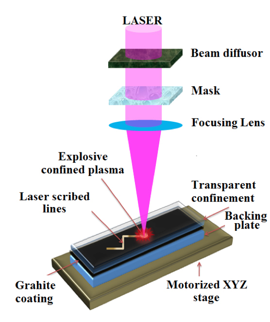
This illustration depicts a new technique that uses a pulsing laser to create synthetic nanodiamond films and patterns from graphite, with potential applications from biosensors to computer chips. (Purdue University image/Gary Cheng)
“The biggest advantage is that you can selectively deposit nanodiamond on rigid surfaces without the high temperatures and pressures normally needed to produce synthetic diamond,” said Gary Cheng, an associate professor of industrial engineering at Purdue University. “We do this at room temperature and without a high temperature and pressure chamber, so this process could significantly lower the cost of making diamond. In addition, we realize a direct writing technique that could selectively write nanodiamond in designed patterns.”
The ability to selectively “write” lines of diamond on surfaces could be practical for various potential applications including biosensors, quantum computing, fuel cells and next-generation computer chips.
The technique works by using a multilayered film that includes a layer of graphite topped with a glass cover sheet. Exposing this layered structure to an ultrafast-pulsing laser instantly converts the graphite to an ionized plasma and creates a downward pressure. Then the graphite plasma quickly solidifies into diamond. The glass sheet confines the plasma to keep it from escaping, allowing it to form a nanodiamond coating.
“These are super-small diamonds and the coating is super-strong, so it could be used for high-temperature sensors,” Cheng said.
Research findings are detailed in a paper that appeared online in the Nature journal Scientific Reports. The paper was authored by former Purdue doctoral students Yuefeng Wang, Yingling Yang, Ji Li and Martin Y. Zhang; postdoctoral research associate Jiayi Shao; doctoral students Qiong Nian and Liang Tang; and Cheng.
The researchers made the discovery while studying how to strengthen metals using a thin layer of graphite and a nanosecond-pulsing laser. A doctoral student noticed that the laser was either causing the graphite to disappear or turn semi-transparent.
“The black coating of graphite was gone, but where did it go?” Cheng said.
Subsequent research proved the graphite had turned into diamond. The Purdue researchers have named the process confined pulse laser deposition (CPLD).
The research team confirmed that the structures are diamond using a variety of techniques including transmission electron microscopy, X-ray diffraction and the measurement of electrical resistance.
A U.S. patent application has been filed on the concept through the Purdue Office of Technology Commercialization. More research is needed to commercialize the technique, Cheng said.
Writer: Emil Venere, 765-494-4709, venere@purdue.edu
Source: Gary J. Cheng, 765-494-5436, gjcheng@purdue.edu
ABSTRACT
Direct Laser Writing of Nanodiamond Films from Graphite under Ambient Conditions
Qiong Nian, Yuefeng Wang, Yingling Yang, Ji Li, Martin Y. Zhang, Jiayi Shao, Liang Tang & Gary J. Cheng
Purdue University
Synthesis of diamond, a multi-functional material, has been a challenge due to very high activation energy for transforming graphite to diamond, and therefore, has been hindering it from being potentially exploited for novel applications. In this study, we explore a new approach, namely confined pulse laser deposition (CPLD), in which nanosecond laser ablation of graphite within a confinement layer simultaneously activates plasma and effectively confine it to create a favorable condition for nanodiamond formation from graphite. It is noteworthy that due to the local high dense confined plasma created by transparent confinement layer, nanodiamond has been formed at laser intensity as low as 3.7 GW/cm2, which corresponds to pressure of 4.4 GPa, much lower than the pressure needed to transform graphite to diamond traditionally. By manipulating the laser conditions, semi-transparent carbon films with good conductivity (several kΩ/Sq) were also obtained by this method. This technique provides a new channel, from confined plasma to solid, to deposit materials that normally need high temperature and high pressure. This technique has several important advantages to allow scalable processing, such as high speed, direct writing without catalyst, selective and flexible processing, low cost without expensive pico/femtosecond laser systems, high temperature/vacuum chambers.
Media Contact
All latest news from the category: Process Engineering
This special field revolves around processes for modifying material properties (milling, cooling), composition (filtration, distillation) and type (oxidation, hydration).
Valuable information is available on a broad range of technologies including material separation, laser processes, measuring techniques and robot engineering in addition to testing methods and coating and materials analysis processes.
Newest articles

First-of-its-kind study uses remote sensing to monitor plastic debris in rivers and lakes
Remote sensing creates a cost-effective solution to monitoring plastic pollution. A first-of-its-kind study from researchers at the University of Minnesota Twin Cities shows how remote sensing can help monitor and…

Laser-based artificial neuron mimics nerve cell functions at lightning speed
With a processing speed a billion times faster than nature, chip-based laser neuron could help advance AI tasks such as pattern recognition and sequence prediction. Researchers have developed a laser-based…

Optimising the processing of plastic waste
Just one look in the yellow bin reveals a colourful jumble of different types of plastic. However, the purer and more uniform plastic waste is, the easier it is to…


