NRL develops laser processing method to increase efficiency of optoelectronic devices

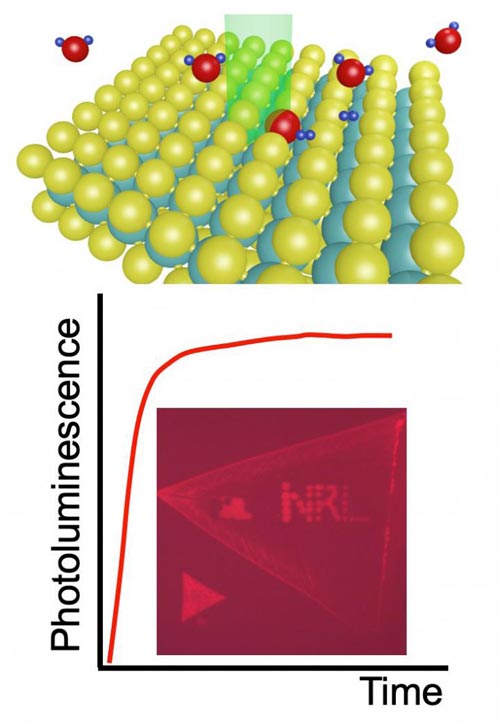
(Top) Illustration of a water molecule bonding at a sulfur vacancy in the MoS2 upon laser light exposure. (Bottom) Photoluminescence (PL) increase observed during laser light exposure in ambient. (Inset) Fluorescence image showing brightened regions spelling out 'NRL.' Credit: U.S. Naval Research Laboratory
“From a chemistry standpoint, we have discovered a new photocatalytic reaction using laser light and water molecules, which is new and exciting,” said Saujan Sivaram, Ph.D., lead author of the study. “From a general perspective, this work enables the integration of high quality, optically active, atomically thin material in a variety of applications, such as electronics, electro-catalysts, memory, and quantum computing applications.”
The NRL scientists developed a versatile laser processing technique to significantly improve the optical properties of monolayer molybdenum disulphide (MoS2) — a direct gap semiconductor — with high spatial resolution.
Their process produces a 100-fold increase in the material's optical emission efficiency in the areas “written” with the laser beam.
According to Sivaram, atomically thin layers of transition metal dichalcogenides (TMDs), such as MoS2, are promising components for flexible devices, solar cells, and optoelectronic sensors due to their high optical absorption and direct band gap.
“These semiconducting materials are particularly advantageous in applications where weight and flexibility are a premium,” he said. “Unfortunately, their optical properties are often highly variable and non-uniform making it critical to improve and control the optical properties of these TMD materials to realize reliable high efficiency devices.”
“Defects are often detrimental to the ability of these monolayer semiconductors to emit light,” Sivaram said. “These defects act as non-radiative trap states, producing heat instead of light, therefore, removing or passivating these defects is an important step towards high efficiency optoelectronic devices.”
In a traditional LED, approximately 90 percent of the device is a heat sink to improve cooling. Reduced defects enable smaller devices to consume less power, which results in a longer operational lifetime for distributed sensors and low-power electronics.
The researchers demonstrated that water molecules passivate the MoS2 only when exposed to laser light with an energy above the band gap of the TMD. The result is an increase in photoluminescence with no spectral shift.
Treated regions maintain a strong light emission compared to the untreated regions that exhibit much a weaker emission. This suggest that the laser light drives a chemical reaction between the ambient gas molecules and the MoS2.
“This is a remarkable achievement,” said Berend Jonker, Ph.D., senior scientist and principal investigator. “The results of this study pave the way for the use of TMD materials critical to the success of optoelectronic devices and relevant to the Department of Defense mission.”
###
The research team includes Saujan Sivaram, Ph.D.; Aubrey Hanbicki, Ph.D.; Matthew Rosenberger, Ph.D.; Hsun-Jen Chuang, Ph.D.; Kathleen McCreary, Ph.D.; and Berend Jonker, Ph.D., from the NRL Materials Science and Technology Division, and Glenn Jernigan, Ph.D., from the NRL Electronics Science and Technology Division. Sivaram and Rosenberger hold National Research Council (NRC) fellowships at NRL. Chuang holds an American Society for Engineering Education (ASEE) fellowship at NRL. The research results are reported in ACS Applied Materials & Interfaces; DOI: 10.1021/acsami.9b00390.
Media Contact
All latest news from the category: Process Engineering
This special field revolves around processes for modifying material properties (milling, cooling), composition (filtration, distillation) and type (oxidation, hydration).
Valuable information is available on a broad range of technologies including material separation, laser processes, measuring techniques and robot engineering in addition to testing methods and coating and materials analysis processes.
Newest articles

Compact LCOS Microdisplay with Fast CMOS Backplane
…for High-Speed Light Modulation. Researchers from the Fraunhofer Institute for Photonic Microsystems IPMS, in collaboration with HOLOEYE Photonics AG, have developed a compact LCOS microdisplay with high refresh rates that…

New perspectives for material detection
CRC MARIE enters third funding period: A major success for terahertz research: Scientists at the University of Duisburg-Essen and the Ruhr University Bochum have been researching mobile material detection since…

CD Laboratory at TU Graz Researches New Semiconductor Materials
Using energy- and resource-saving methods, a research team at the Institute of Inorganic Chemistry at TU Graz aims to produce high-quality doped silicon layers for the electronics and solar industries….


